Table 7-21, Pcie switch control and status 2 register - 0x19, Fpga registers – Artesyn iVPX7225 Installation and Use (April 2015) User Manual
Page 135
FPGA Registers
iVPX7225 Installation and Use (6806800S11C)
116
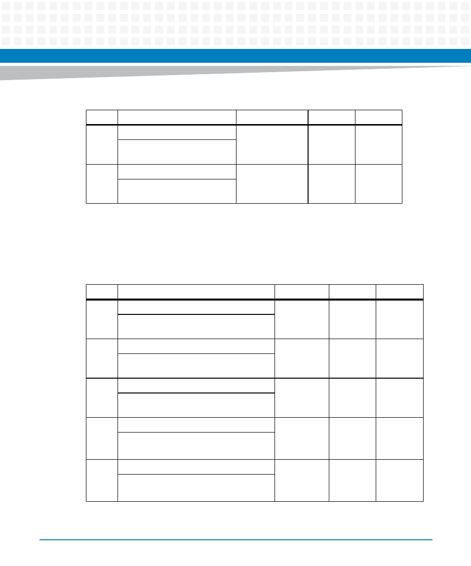
7.1.21 PCIE Switch Control and Status 2 Register - 0x19
6
Interrupt Output
Ext.
RO
-
0: Interrupt asserted
1: Interrupt de-asserted
7
Fatal Error Detection
Ext.
RO
-
0: Fatal error detected
1: No fatal error detected
Table 7-20 PCIE Switch Control and Status 1 Register - 0x18
Bit #
Description
Default
LPC Access
I2C Access
Table 7-21 PCIE Switch Control and Status 2 Register - 0x19
Bit #
Description
Default
LPC Access
I2C Access
0
Non-transparent Mode Enable
1
R/W
-
0: NT mode enabled
1: NT mode disabled
1
Non-transparent PCI-PCI Bridge Enable
1
R/W
-
0: NT PCI-PCI bridge enabled
1: NT PCI-PCI bridge disabled
2
System SMBus Interface Enable
0
R/W
-
0: Interface enabled
1: Interface disabled
3
Spread Spectrum Clocking Crossing Enable
1
R/W
-
0: SSC crossing enabled
1: SSC crossing disabled
4
Link Upconfigure Timer Enable
1
R/W
-
0: Timer enabled
1: Timer disabled