Table 7-32, Super io logical device number register, Table 7-33 – Artesyn iVPX7225 Installation and Use (April 2015) User Manual
Page 142: Super io device identification register, Table 7-34, Super io device revision register, Fpga registers
FPGA Registers
iVPX7225 Installation and Use (6806800S11C)
123
0x28
Super IO LPC Control
0x29
Super IO SERIRQ
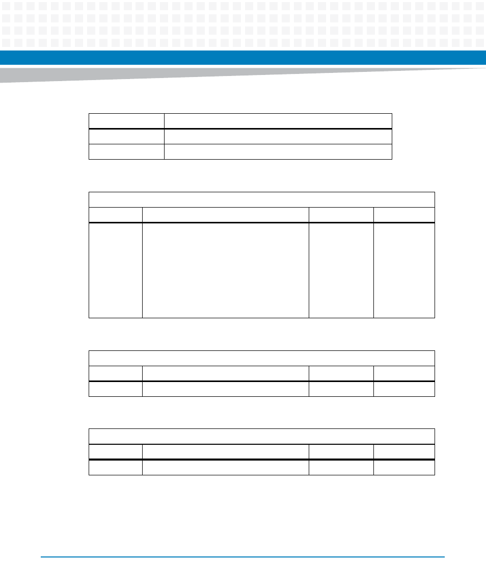
Table 7-32 Super IO Logical Device Number Register
Index Address: 0x07
Bit #
Description
Default
Access
7:0
Logical Device Number:
0x04: Logical Device 4 (UART 1Serial Port 1)
0x05: Logical Device 5 (UART 2 Serial Port 2)
0x06: Logical Device 6 (UART 3Serial Port 3)
A write to this register selects the current
logical device. This allows access to the control
and configuration registers for each logical
device.
0
LPC: R/W
Table 7-33 Super IO Device Identification Register
Index Address: 0x20
Bit #
Description
Default
Access
7:0
Device ID
0
LPC: R
Table 7-34 Super IO Device Revision Register
Index Address: 0x21
Bit #
Description
Default
Access
7:0
Device Revision
0x01
LPC: R
Table 7-31 Global Configuration Register Summary (continued)
Index Address
Description