BECKHOFF BK3000 User Manual
Page 40

Appendix
40
BK3xxx/LC3100
Input data
in the bus coupler
I0
...
byte-oriented data
...
I3
I4
...
bit-oriented data
...
I5
The base addresses I0 and O0 listed here are used as relative addresses
or addresses in the bus coupler. If you have an appropriate superordinate
Profibus system you can use the bus master to enter these addresses at
any desired position in the process image of the control unit. You can use
the configuration software of the master to assign the bytes to the
addresses in the process image of the control unit.
Representation of analog signals in the process image
In the standard case, the analog signals are presented as follows: to input
bytes or to output bytes of the process image are needed for each analog
channel. The two bytes represent the value as unsigned interger, i.e. 15
bits with the sign. The data format is used independently of the actual
resolution. Example: with a resolution of 12 bits in the case of analog
values in the positive and negative value ranges, the four least significant
bits are of no importance. If the value of the analog signal is only positive,
the sine bit (bit 15, MSB) is always "0". In this case, the 12 bits of the
analog value are represented in bit 14 to bit 3. The three least significant
bits are of no importance.
By configuration via the Profibus master software or the KS2000 software,
the bus coupler can represent all or individual analog channels in an
extended mode. Optionally, the control and status byte of a channel can
also be inserted. The least significant byte of three bytes has control and
status functions. The other two bytes become inputs and outputs. Various
operating modes can be set with the control byte. The 6 least significant
bits of the control and status byte can be used as addressing bits.
Addressing serves to read and write a register set inside the terminal. The
register set has 64 registers. The settings are stored permanently.
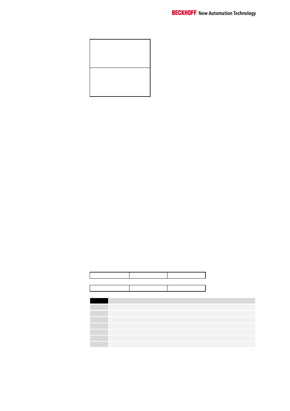
I/O bytes of an analog
Output byte 1
Output byte 0
Control byte
channel in the process
image
Input byte 1
Input byte 0
Status byte
Significance of the
BIT 7
0 = NORMAL MODE,
1 = CONTROL MODE
control/status bytes
BIT 6
0 = READ,
1 = WRITE
for accessing
BIT 5
Register address, MSB
the register model
BIT 4
Register address
BIT 3
Register address
BIT 2
Register address
BIT 1
Register address
BIT 0
Register address, LSB