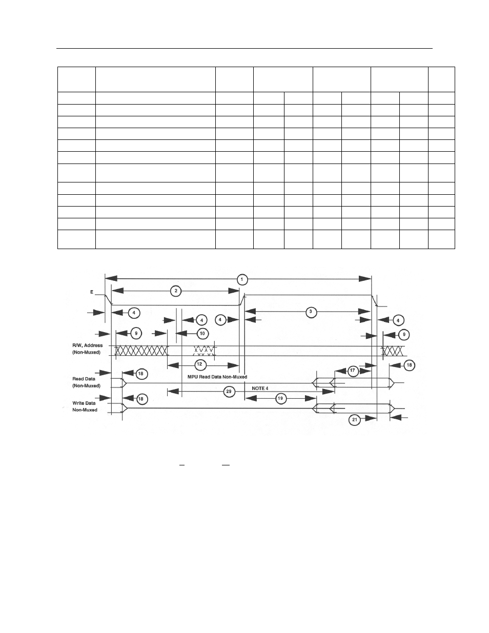
Figure 2-3. read/write timing diagram – Fluke Biomedical 942A-200L-M4 User Manual
Page 20
942A-200L-M4 & 942A-200L-M5 UDR
Operator Manual
2-6
Table 2-1. Bus Timing Characteristics
Ident.
Number
Characteristics Symbol
MC6802NS
MC6802
MC6808
MC68A02
MC68A08
MC68B02
MC68B08
Unit
Min Max Min Max Min
Max
1 Cycle
Time
t
cyc 1.0 10 0.667
10 0.5 10 µs
2
Pulse Width, E Low
PW
EL
450 5000 280 5000 210 5000 ns
3
Pulse Width, E High
PW
EH
450 9500 280 9700 220 9700 ns
4
Clock Rise and Fall Time
t
r,
t
f --- 25 --- 25 --- 20 ns
9
Address Hold Time
t
AH 20 --- 20 --- 20 --- ns
12
Non-Muxed Address Valid
Time
t
AV1
t
AV2
16
---
---
270
100
---
---
---
50
---
---
---
ns
17
Read Data Setup Time
t
DSR 100 --- 70 --- 60 --- ns
18
Read Data Hold Time
t
DHR
10 --- 10 --- 10 --- ns
19
Write Data Delay Time
t
DDW
--- 225 --- 170 --- 160 ns
21
Write Data Hold Time
t
DHW
30 --- 20 --- 20 --- ns
29
Usable Access Time (See Note
4)
t
ACC
605 --- 310
--- 235
--- ns
NOTES:
1. Voltage levels shown are
v
L
<
0.4 V
,
V
H
<
2.4 V,
unless otherwise specified.
2. Measurement points shown are 0.8 V and 2.0 V, unless otherwise noted.
3. All electricals shown for the MC6802 apply to the MC6802NS and MC6808, unless otherwise
noted.
4. Usable access time is computed by: 12 + 3 + 4 - 17.
5. If programs are not executed from on-board RAM, TAV1 applies. If programs are to be stored and
executed from on-board RAM, TAV2 applies. For normal data storage in the on-board RAM, this
extended delay does not apply. Programs cannot be executed from on-board RAM when using A
and B parts (MC68A02, MC68A08, MC68B02, MC68B08). ON-board RAM can be used for data
storage with all parts.
Figure 2-3. Read/Write Timing Diagram