U14 pin – Fluke Biomedical 942A-200L-M4 User Manual
Page 22
942A-200L-M4 & 942A-200L-M5 UDR
Operator Manual
2-8
Data transceiver U73 provides buffer and drive capability to the external data bus interface, available for
optional circuit boards on J3. Data direction is controlled by the read/write (/R/W) line on U73-11
providing U73-9 (/BUS ENABLE) is low, which enables port-to-port data transfer to occur. The bus
enable signal is generated by the option board/boards when they are addressed by the MPU. When U73-
11 is low, for a read cycle, data is transferred from the external bus to the internal bus. When U73-11 is
high, for a write cycle, data is transferred from the internal bus to the external bus.
Control Signal Buffer
Line driver U18 provides a signal drive for all system control signals and clocks utilized by circuitry within
the main circuit board.
Line driver U74 provides the drive for control lines and clock signals for external circuitry utilizing the J3
option interlace connector.
Address Decoding
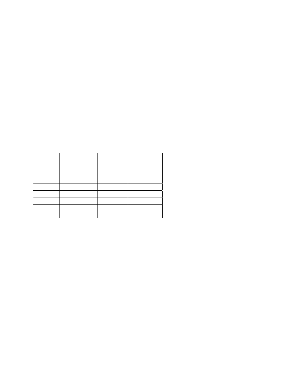
The master decoder (U14) is an open-collector 32 x 8-bit bipolar PROM. Address lines A15, A14, A13,
and A12 as well as read/write (/R/W) used to decode memory and I/O addresses in 4K hex blocks. Table
2-2 lists the output signals from U 14.
Table 2-2. Output Signals (U14)
U14 Pin
Signal Name
Address
Read/Write
9
/PROM 8000
8000-FFFF
Read Only
7 /SPARE
Spare
6 /RAM
2000
2000-3FFF
Read/Write
5
/ RAM 0000
0000-1FFF
Read/Write
4 /I/O
4000-4FFF
Read/Write
3
/RAM WRITE
0000-3FFF
Write Only
2
/RAM READ
0000-3FFF
Read Only
1 /5000
BLOCK
5000-5FFF
Read/Write
/PROM 8000 directly drives the enable pins of the PROM. RAM 0000, RAM 2000 and RAM READ are
logic OR’d with /CLOCK by U17. /RAM READ drives the RAM output. /RAM 0000 and /RAM 2000 act
as chip enables for the appropriate RAM. /RAM WRITE is logic OR’d with /WRITE 02 by U17, which is
connected to the write enable pins on the rams. The /5000 BLOCK output signal is applied to driver U74
and connected to J3, the optional interface buss connector.
The /I/O output signal is applied to major function decoder U1 that is a 1 of 8 decoder. U1 utilizes
address lines A5, A6, A7, and A8 as well as CLOCK to generate outputs that are decoded in 32 hex
blocks starting at address 4000. Table 2-3 lists U1 outputs, their functions and addresses.