Address state, Hex address, Function – Fluke Biomedical 942A-200L-M4 User Manual
Page 28
942A-200L-M4 & 942A-200L-M5 UDR
Operator Manual
2-14
Digital to Analog Converter and Output Circuitry (Write Only)
The D/A converter (U82) is an 8-bit buffered multiplying device that responds to address 4004. Data is
written and latched by U82 when /DAC, /CS and /WR are active (low). The converter is configured for
unipolar operation with a voltage reference of + 10VDC. Below is the digital to analog conversion table
with the voltage measured at U82-1 referenced to ground.
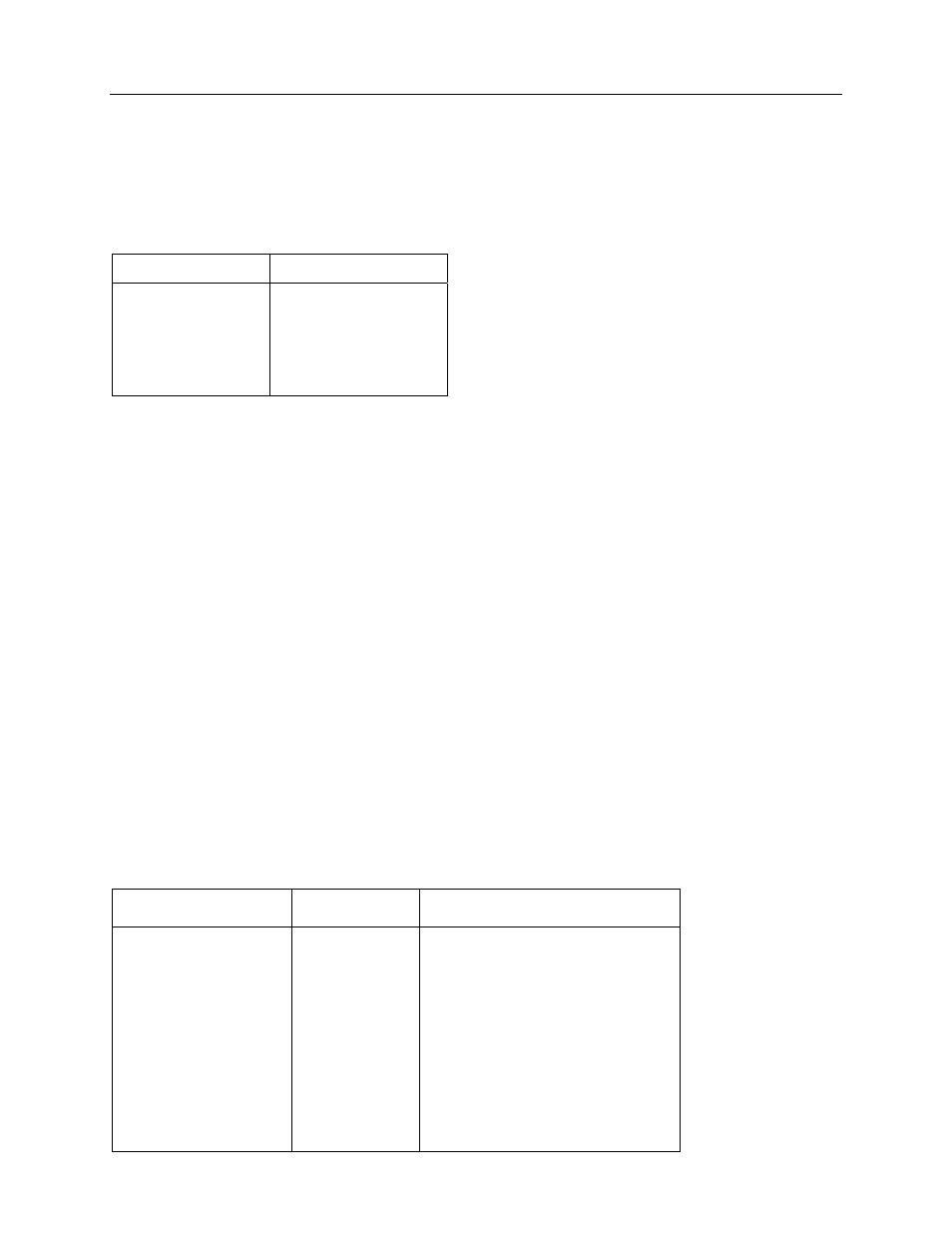
Table 2-10. Digital to Analog Conversion
MSB LSB ANALOG
OUTPUT
1111 1111
-10
VDC
1000 0000
-5
VDC
0000 0001
-0.039
V
0000 0000
0
V
U81 operational amplifier 1 buffers the converter output to drive the three analog output circuits. This
voltage is also provided to J4, analog option connector. J4 is provided with the necessary supply
voltages to configure a custom analog output range for special applications (i.e. 10 mV to 50 mV). U81
operational amplifier 3 provides the user with a 0 - 10 volt analog output. VR1 is the zero adjustment and
VR2 is the span adjustment for the 0 - 10 volts output.
The circuitry comprised of U80 operational amplifiers 1 and 2, as well as U81 operational amplifier 2,
provides a 4 - 20 mA user output. VR7 is adjusted to obtain a 4 mA reading on the output, and VR4 is
adjusted to obtain a 20 mA reading on the output. U81 operational amplifier 2 and Q1 are configured as
a constant current source controlled by the output of U80 operational amplifier 1. The positive feedback
circuitry, comprised of R41 and R43, ensures that the output current will remain constant regardless of
the output load impedance. The maximum load impedance is 500 ohms.
The circuitry comprised of U80 operational amplifiers 3 and 4 as well as U81 operational amplifier 4
provides a second 4 - 20 mA user output. Operation is identical to the circuitry previously described in
this section. VR6 is adjusted to obtain a 4 mA reading at the output and VR5 is adjusted to obtain a 20
mA reading at the output.
Read Register Decoding
Decoding for READ registers within the main circuit board is performed by U34, which is a 1 of 8 decoder.
Control signals for U34 are /REGSELECT, and /R/W (active high) as well as address A1, A2, and A3.
U34 decodes address per output, starting with 4000 and ending with 400E.
These outputs are active low. Table 2-10 lists the READ register, the assigned function and the address.
Table 2-11. Control Signal Address Decoding (U34)
Address State
A3 A2
A1
Hex Address
Function
0 0
0
4000
Switch
Interface
0 0
1
4002
Data
Entry
0
1
0
4004
Gross Counter Low
0
1
1
4006
Gross Counter High
1 0
0
4008
Sensitivity
Select
1 0
1
400A
(Spare)
1 1
0
400C
(Spare)
1 1
1
400E
(Spare)