Scsi transfer (sxfer), Scsi transfer, Sxfer) – Avago Technologies LSI53C825AE User Manual
Page 119
Operating Registers
4-31
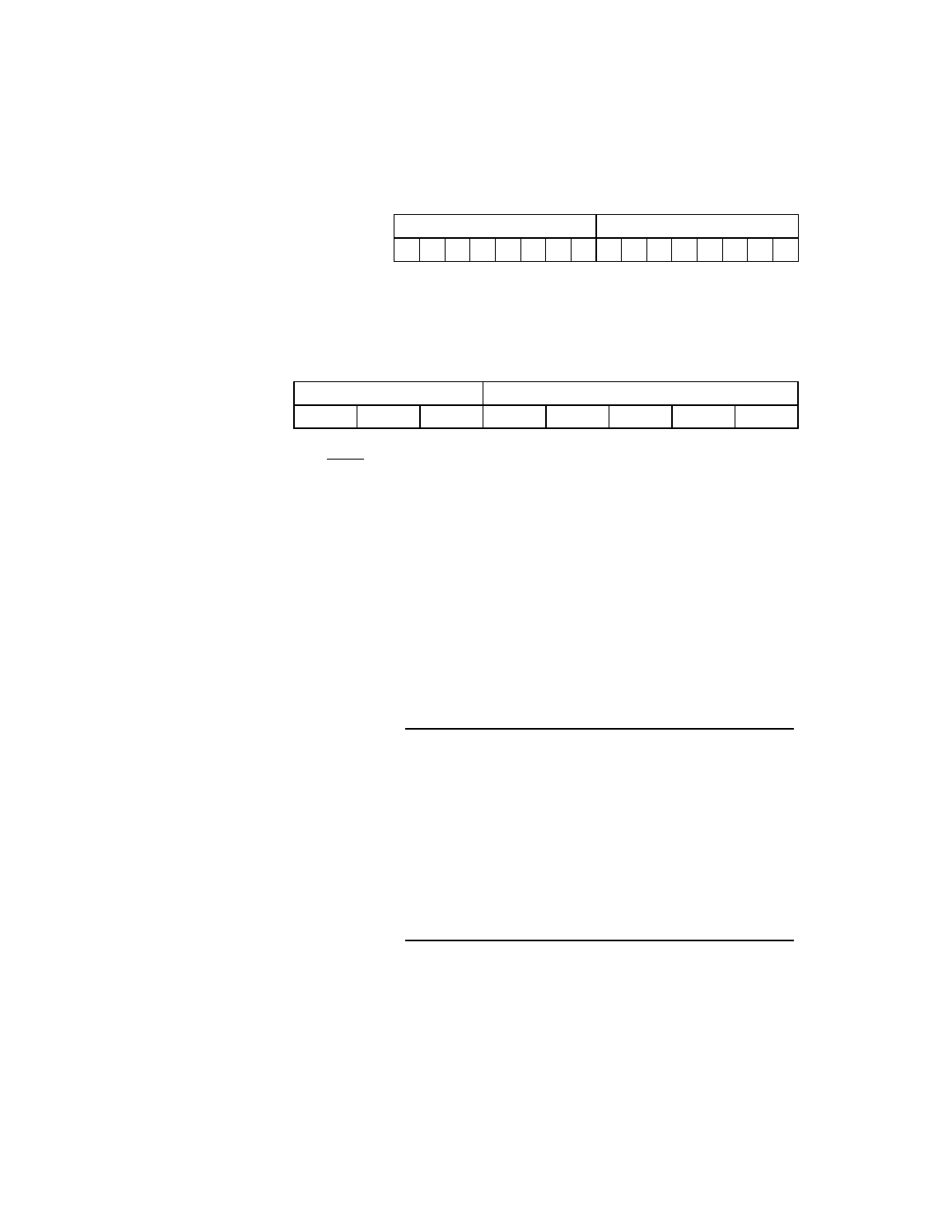
Register: 0x05 (0x85)
SCSI Transfer (SXFER)
Read/Write
Note:
When using Table Indirect I/O commands, bits [7:0] of this
register are loaded from the I/O data structure.
For additional information on how the synchronous transfer
rate is determined, refer to
Chapter 2, “Functional Descrip-
TP[2:0]
SCSI Synchronous Transfer Period
[7:5]
These bits determine the SCSI synchronous transfer
period used by the LSI53C825A when sending
synchronous SCSI data in either the initiator or target
mode. These bits control the programmable dividers in
the chip.
The synchronous transfer period the LSI53C825A should
use when transferring SCSI data is determined in the
following example:
Highest
Lowest
7
6
5
4
3
2
1
0
15 14 13 12 11 10
9
8
7
5
4
0
TP[2:0]
MO[4:0]
0
0
0
0
0
0
0
0
TP2
TP1
TP0
XFERP
0
0
0
4
0
0
1
5
0
1
0
6
0
1
1
7
1
0
0
8
1
0
1
9
1
1
0
10
1
1
1
11