Chip test six, Ctest6) – Avago Technologies LSI53C825AE User Manual
Page 149
Operating Registers
4-61
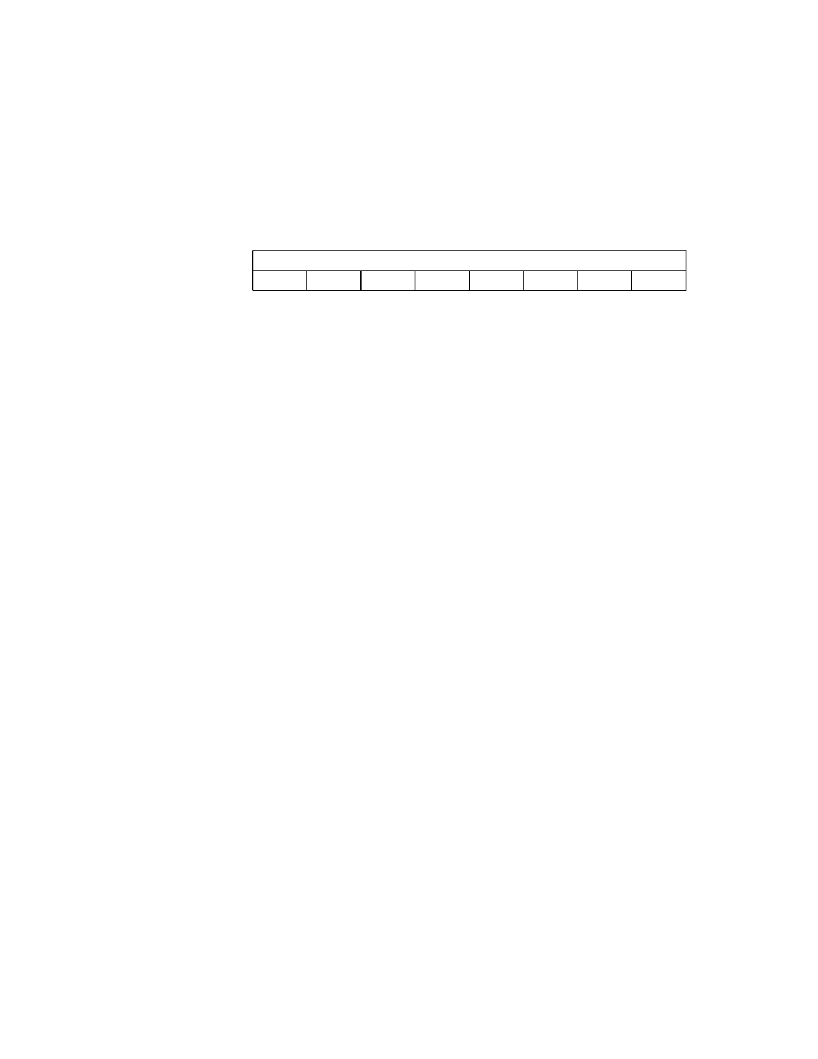
Register: 0x23 (0xA3)
Chip Test Six (CTEST6)
Read/Write
DF
DMA FIFO
[7:0]
Writing to this register writes data to the appropriate byte
lane of the DMA FIFO as determined by the FBL bits in
the
register. Reading this
register unloads data from the appropriate byte lane of
the DMA FIFO as determined by the FBL bits in the
register. Data written to the FIFO is
loaded into the top of the FIFO. Data read out of the FIFO
is taken from the bottom. To prevent DMA data from
being corrupted, this register should not be accessed
before starting or restarting SCRIPTS operation. Write to
this register only when testing the DMA FIFO using the
register. Writing to this register
while the test mode is not enabled produces unexpected
results.
7
0
DF
0
0
0
0
0
0
0
0