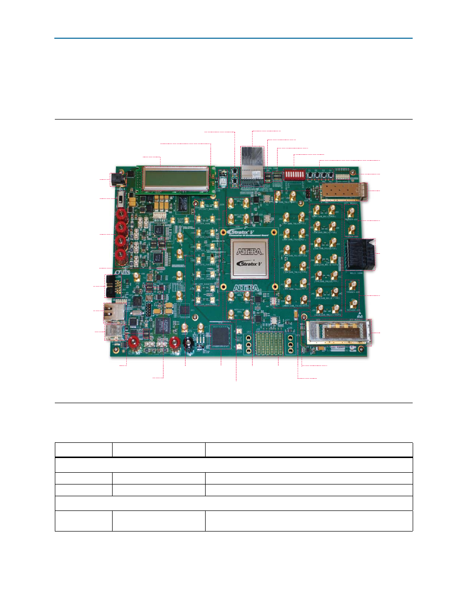
Board overview, Board overview –2, Figure 2–1 – Altera Transceiver Signal Integrity Development Kit, Stratix V GT Edition User Manual
Page 10: Table 2–1
2–2
Chapter 2: Board Components
Board Overview
Transceiver Signal Integrity Development Kit
May 2014
Altera Corporation
Stratix V GT Edition Reference Manual
Board Overview
This section provides an overview of the Stratix V GT transceiver signal integrity
development board, including an annotated board image and component
descriptions.
provides an overview of the development board features.
describes the components and lists their corresponding board references.
Figure 2–1. Overview of the Stratix V GT Transceiver Signal Integrity Development Board Features
User DIP Switch (SW4)
Stratix V GT
FPGA (U29)
VCCRT_GXB/ VCCA_GXB
Voltage Select (SW2)
MSEL Selection/MAX II Bypass (S7)
Clock Trigger
Outputs
(U32, U33)
Clock Trigger
Outputs
(U34, U35)
Transceiver Clock Input Select DIP switch (SW6)
Reset Push Buttons (S5, S6)
MAX II
CPLD (U19)
MMPX
Connectors
Transceiver Input
Reference Clocks
User Push
Buttons
(SW1-SW4)
User LEDs
(D8-D15)
SFP+
Module
(J51)
XFP Module
(U25)
Molex
Backplane
Connector
(J34)
Tyco
Connector
(J33)
Amphenol Backplane Connector (J32)
Power
Switch
(SW1)
JTAG Header
(J93)
DC Power
Jack (J1)
Character LCD (J30)
Embedded
USB-Blaster
(CN1)
Power Sequence
Enable/Disable
(SW7, SW3)
10/100 /1000
Ethernet
Port (J29)
Fan Connector (J12)
Fan Jumper (J26)
Fan LED (D6)
GXB Receive SMA
GXB Transmit SMA
FPGA Clock Input Select/
Spread Spectrum Clock Select
(SW5)
External Power
Input Banana Jacks
(J6, J15, J18, J21)
Table 2–1. Transceiver Signal Integrity Development Kit Components (Part 1 of 4)
Board Reference
Type
Description
Featured Devices
U29
FPGA
Stratix V GT FPGA (5SGTMC7K2F40C2), 1517-pin BGA.
U19
CPLD
MAX II CPLD (EPM2210F256C3N), 256-pin BGA.
Configuration, Status, and Setup Elements
S7 (pin 6-7)
MAX II bypass switch
Enables or disables the MAX II CPLD in the JTAG chain. The MAX II
CPLD is disabled by default.