Power measurement, Power measurement –39 – Altera Transceiver Signal Integrity Development Kit, Stratix V GT Edition User Manual
Page 47
Chapter 2: Board Components
2–39
Power Supply
May 2014
Altera Corporation
Transceiver Signal Integrity Development Kit
Stratix V GT Edition Reference Manual
Power Measurement
There are six voltage rails tied to two LTC2978 power monitor devices. These devices
are capable of measuring the voltage and current for each voltage rail and also
provide power sequencing. A sense resistor at each voltage rail is in place for these
measurements. These devices are capable of trimming the output voltage ±10%. An
I
2
C bus connects to the MAX II CPLD and FPGA devices for control.
lists the voltage rails. Each voltage is identified by its schematic signal
name.
The LTC2978 power monitor devices on this board are programmed with a project file
that sets up each voltage rail according to a sequence. Each voltage rail adjusts its
voltage level to within a certain tolerance. These two voltage rails can be adjusted
using switch SW2.
lists the VCCRT_GXB and VCCA_GXB voltage rails and their voltage level
depending on the switch position.
1
If you power off and power on the board again with SW2 in the open position, the
voltages for VCCRT_GXB and VCCA_GXB voltage rails read 0.90 V and 2.5 V respectively
and will not come up to the proper levels. This is due to the LTC2978 device trying to
adjust these rails to their programed values, which it cannot due to the switch
position of SW2. The work around to this issue is to set switch SW2 in the close
position at power up.
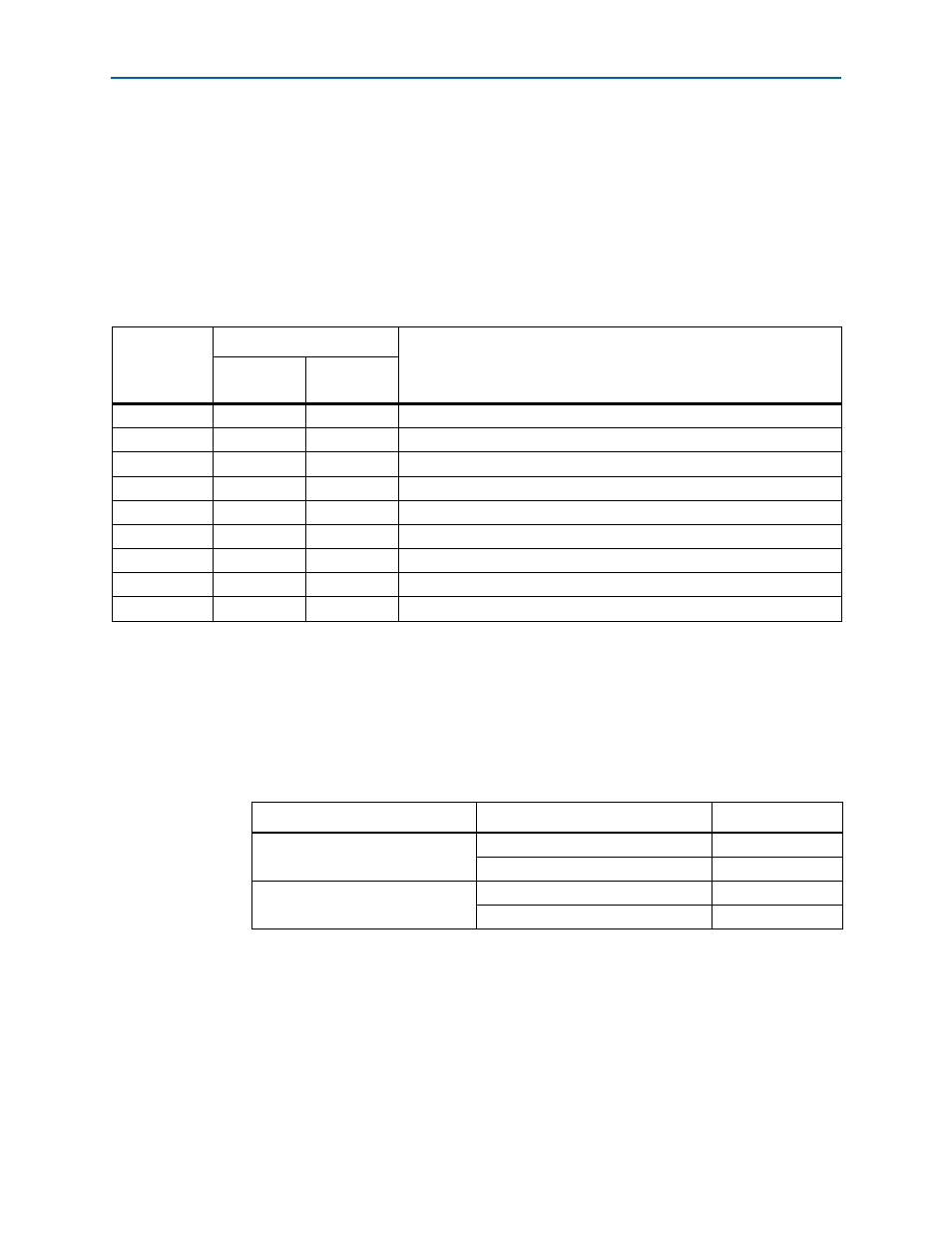
Table 2–40. Voltage Rails
Schematic
Signal Name
Voltage (V)
Description
Production
Silicon
Engineering
Silicon
S5GX_VCC
0.85
0.9
VCC, VCCHIP, VCCHSSI FPGA core power.
VCCR_GTB
0.85 or 1.0
1.1
Transceiver receiver power for 28G channels.
VCCT_GTB
0.85 or 1.0
1.1
Transceiver transmit power for 28G channels.
VCCL_GTB
0.85 or 1.0
1.1
Transceiver clocking power for 28G channels.
VCCRT_GXB
0.85 or 1.0
1.2
Shared VCCR_GXB and VCCT_GXB transceiver power for 12.5G channels.
VCCA_GXB
2.5 or 3.0
3.3
VCCA_GXB transceiver power.
VCCH_GXB
—
1.6
VCCH_GXB transceiver power.
VCCD_FPLL
—
1.6
PLL power.
VCCPT
—
1.6
FPGA power.
Table 2–41. Voltage Level Setting
Switch SW2 (Position 1 and 2)
Schematic Net Name
Voltage (V)
Close (Default)
VCCRT_GXB
1.0
VCCA_GXB
3.0
Open
VCCRT_GXB
0.9
VCCA_GXB
2.5