Altera Transceiver Signal Integrity Development Kit, Stratix V GT Edition User Manual
Page 16
2–8
Chapter 2: Board Components
Featured Device: Stratix V GT FPGA
Transceiver Signal Integrity Development Kit
May 2014
Altera Corporation
Stratix V GT Edition Reference Manual
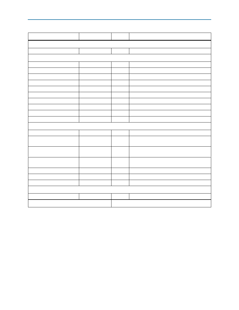
LCD
16 Character × 2 Line LCD
5.0-V LVTTL output
11
LCD
Ethernet
TXD[3:0]
2.5-V CMOS output
4
Ethernet transmit RGMII data bus
TXEN
2.5-V CMOS output
1
Ethernet transmit enable
GTXCLK
2.5-V CMOS output
1
Ethernet transmit clock
RXD[3:0]
2.5-V CMOS input
4
Ethernet receive RGMII data bus
RXDV
2.5-V CMOS input
1
Receive data valid
RXCLK
2.5-V CMOS input
1
Receive clock
MDC
2.5-V CMOS input
1
Ethernet MII clock
MDIO
2.5-V CMOS inout
1
Ethernet MII data
ENET_SGMII_TXP/N
LVDS output
2
Ethernet SGMII transmit data positive/negative
ENET_SGMII_RXP/N
LVDS input
2
Ethernet SGMII receive data positive/negative
Transceivers
28G channels to MMPX
1.4-V PCML
16
Transceiver channel
12.5G channels to Tyco
backplane connector
1.4-V PCML
28
Transceiver channel
12.5G channels to Amphenol
backplane connector
1.4-V PCML
28
Transceiver channel
12.5G channels to Molex
backplane connector
1.4-V PCML
28
Transceiver channel
12.5G channels to SMA
1.4-V PCML
28
Transceiver channel
12.5G channels to a SFP+ cage
1.4-V PCML
4
Transceiver channel
12.5G channels to XFP cage
1.4-V PCML
4
Transceiver channel
Spares
Spare[7:0]
2.5-V CMOS
8
Spare signals to the MAX II CPLD
Device I/O Total:
304
Table 2–4. Stratix V GT I/O Usage Summary (Part 3 of 3)
Function
I/O Type
I/O Count
Description