Development board block diagram, Handling the board – Altera Transceiver Signal Integrity Development Kit, Stratix V GT Edition User Manual
Page 8
1–4
Chapter 1: Overview
Development Board Block Diagram
Transceiver Signal Integrity Development Kit
May 2014
Altera Corporation
Stratix V GT Edition Reference Manual
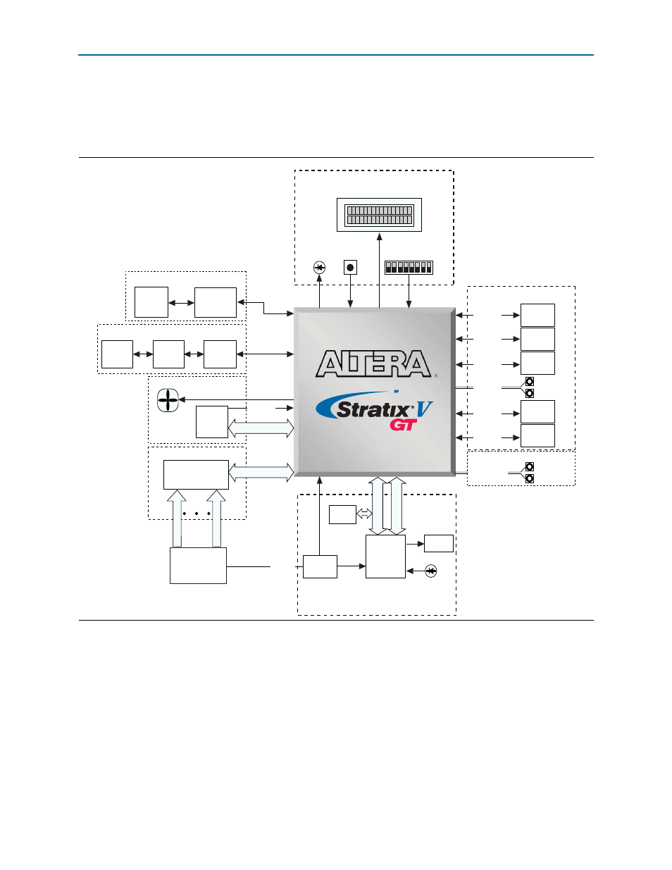
Development Board Block Diagram
shows the block diagram of the Stratix V GT transceiver signal integrity
development board.
Handling the Board
When handling the board, it is important to observe the following static discharge
precaution:
c
Without proper anti-static handling, the board can be damaged. Therefore, use
anti-static handling precautions when touching the board.
The Stratix V GT transceiver signal integrity development board must be stored
between –40º C and 100º C. The recommended operating temperature is between 0º C
and 55º C.
Figure 1–1. Stratix V GT Transceiver Signal Integrity Development Board Block Diagram
LCD
Buttons, Switches, Displays
16 Char × 2 Line LCD
8 User DIP Switch
4 User
Push Buttons
8 User
LEDs
Pwrgood
FPP Configuration
28-Gbps Channels
12.5-Gbps Channels
Clock
Circuitry
Tyco
Connector
1 SFP+
XFP
Amphl/FCI
Connector
28 SMA
Connectors
16 MMPX
Connectors
Molex
Connector
1 Gb
Flash
3 Configuration
Status LEDs
MAX II
EPM2210
CPLD
PGMSEL
Flash
FPP Config
Power Monitor
15-bit ADCs
10-bit IDACs
ADC
2-wire Ch1
Power
Circuitry
2-wire Ch8
Temperature
Dual Temp
Sensor
Temperature Measure
TDIODES
7 TX/RX
1 TX/RX
7 TX/RX
7 TX/RX
1 TX/RX
7 TX/RX
4-ATT TX/RX
5-V Fan
USB-Blaster
USB
Type-B
Connector
FTDI
745BL
USB PHY
MAX II
EPM570M
CPLD
10/100/1000 Ethernet
RJ45+
Magnetics
Marvell
88E1111
Ethernet PHY