Altera Transceiver Signal Integrity Development Kit, Stratix V GT Edition User Manual
Page 12
2–4
Chapter 2: Board Components
Board Overview
Transceiver Signal Integrity Development Kit
May 2014
Altera Corporation
Stratix V GT Edition Reference Manual
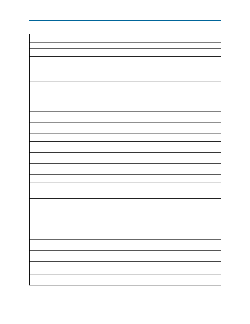
J72 and J73
External core clock output
SMA external output at FPLL/IO4D.
Transceiver Interfaces
J36, J39, J41,
J46, J48, J53,
J55, J57, J59,
J61, J63, J65,
J67, J69
GXB transmit channel
Transceiver GXB transmit channels connected to SMA.
J35, J37, J38,
J40, J42, J45,
J47, J52, J54,
J56, J58, J60,
J62, J64, J66,
J68
GXB receive channel
Transceiver GXB receive channels connected to SMA.
J51
Transceiver optical interface
Transceiver receive and transmit channel connected to the SFP+
module.
U25
Transceiver optical interface
Transceiver receive and transmit channel connected to the XFP
module.
Transceiver Interfaces – Backplane Connectors
J33
10Gbase-KR reference
backplane
7 transceiver-channel pairs, right angle receptacle for Tyco backplane
connector.
J34
10Gbase-KR reference
backplane
7 transceiver-channel pairs, right angle receptacle for Molex Impact
backplane connector.
J32
10Gbase-KR reference
backplane
7 transceiver-channel pairs, right angle receptacle for Amphenol
backplane connector.
Transceiver Interfaces – Stratix V GT
J94, J96, J98,
J100, J102, J104,
J106, J108
Advanced transceiver interface Transceiver GTB receive channels connected to the MMPX connectors.
J95, J97, J99,
J101, J103, J105,
J107, J109
Advanced transceiver interface Transceiver GTB transmit channels connected to the MMPX
connectors.
J110, J111, J112,
J113
Transceiver test trace
Transceiver GTB receive and transmit channels connected to the
MMPX connectors with an eight inch test trace.
General User Input and Output
D18-D25
User LEDs
8 user LEDs. Illuminates when driven low.
SW4
User DIP switch
Octal user DIP switch. When the switch is in the open position, a logic
0 is selected.
S5
Configuration reset push
button
The default reset for the MAX II CPLD System Controller.
S6
CPU reset push button
The default reset for the FPGA logic.
S1-S4
General user push buttons
Four user push buttons. Driven low when pressed.
J30
Character LCD header
A single 14-pin 0.1" pitch dual-row header which interfaces to the 16
character × 2 line LCD module.
Table 2–1. Transceiver Signal Integrity Development Kit Components (Part 3 of 4)
Board Reference
Type
Description