General-purpose clocks, General-purpose clocks –22 – Altera Transceiver Signal Integrity Development Kit, Stratix V GT Edition User Manual
Page 30
2–22
Chapter 2: Board Components
Clock Circuitry
Transceiver Signal Integrity Development Kit
May 2014
Altera Corporation
Stratix V GT Edition Reference Manual
In addition to the four oscillators, each side has a dedicated differential REFCLK input
from a pair of SMA connectors to allow an external clock source.
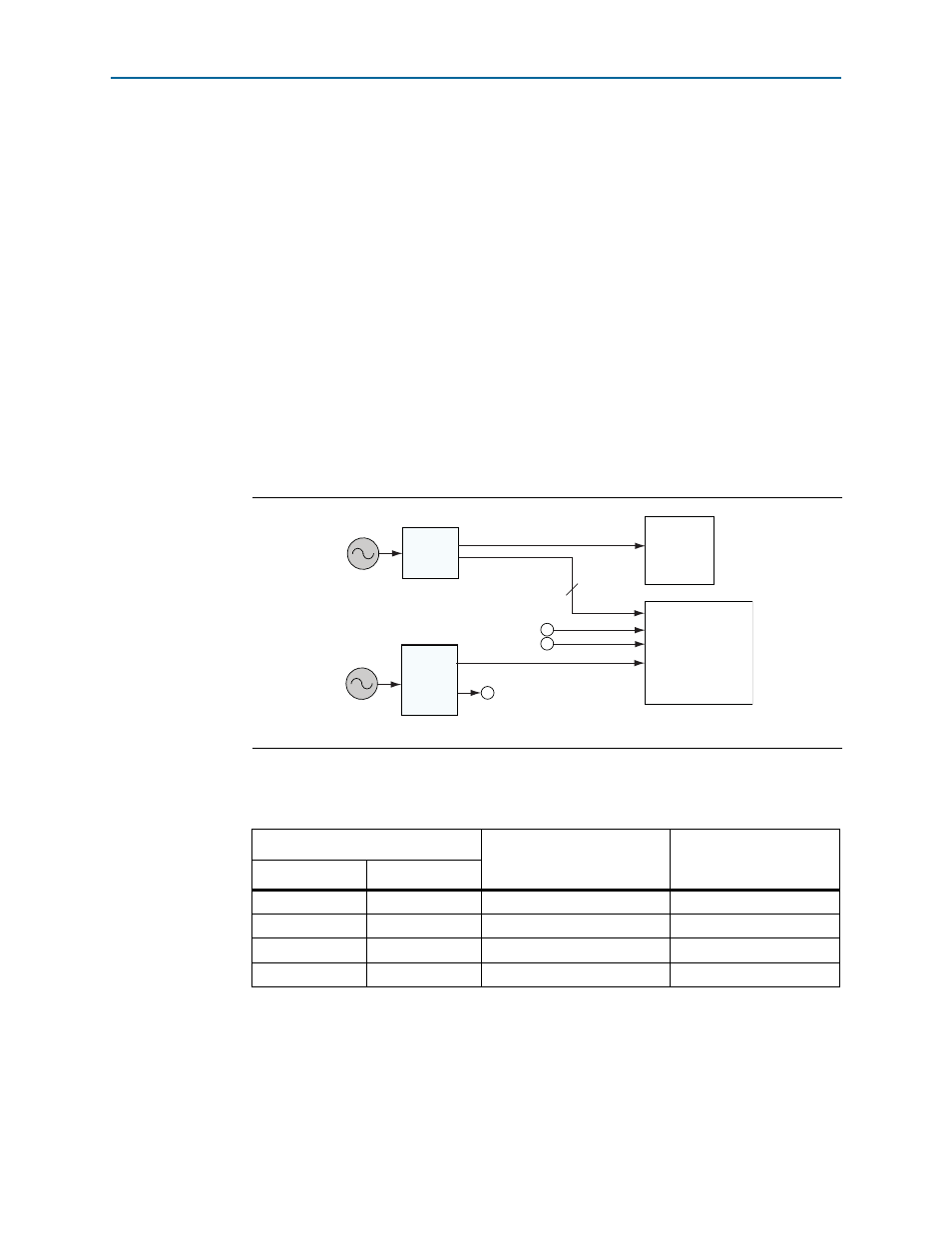
General-Purpose Clocks
Three general-purpose clocks are provided to the FPGA global clock inputs for
general FPGA design. The clocks consist of the following components:
■
A 50-MHz oscillator through an ICS8304 buffer for NIOS II applications at clock
input CLK2p. This clock also routes to the MAX II device for FPP configuration and
to the clock inputs CLK12p and CLK16p of banks 7 and 8.
■
A 25-MHz crystal oscillator through an ICS557-03 spread spectrum differential
clock buffer. The available frequencies and down spread percentages available
from the spread spectrum buffer is shown in
■
An external differential clock source from SMA at CLK10p/n (J70/J71).
shows the general purpose clocks going in to the Stratix V GT transceiver
signal integrity development board.
lists the spread spectrum clock settings and frequencies.
Figure 2–7. Transceiver Signal Integrity Development Kit General Purpose Clocks
Table 2–15. Spread Spectrum Clock Settings and Frequencies
Spread Spectrum Buffer (inputs)
Output Clock Select
Spread (%)
SS1/S1
SS0/S0
0
0
25 MHz (default)
Center
0.25
0
1
100 MHz
Down –0.5
1
0
125 MHz
Down –0.75
1
1
200 MHz
No spread
ICS8304
CLKBUF
MAX II CPLD
(U19)
CLKIN SMA
(J70/J71)
Trigger SMA
ICS557
25/100/125/
200-MHz
Spread
Spectrum
CLKBUF
Stratix V GT
FPGA
(U29)
50 MHz
25 MHz
XTAL
3