Flash memory, Flash memory –36 – Altera Transceiver Signal Integrity Development Kit, Stratix V GT Edition User Manual
Page 44
2–36
Chapter 2: Board Components
Flash Memory
Transceiver Signal Integrity Development Kit
May 2014
Altera Corporation
Stratix V GT Edition Reference Manual
Flash Memory
The development board has a 1-Gb CFI-compatible synchronous flash device for
non-volatile storage of the FPGA configuration data, board information, test
application data, and user code space. The FPGA and MAX II System Controller
shares this device.
This 16-bit data memory interface can sustain burst read operations at up to 52 MHz
for a throughput of 832 Mbps per device. The write performance is 270 µs for a single
word and 310 µs for a 32-word buffer. The erase time is 800 ms for a 128 K parameter
block.
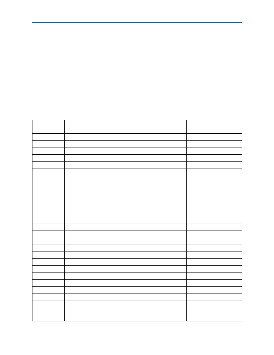
lists the flash pin assignments, signal names, and functions. The signal
names and types are relative to the Stratix V GT device in terms of I/O setting and
direction.
Table 2–37. Flash Pin Assignments, Schematic Signal Names, and Functions (Part 1 of 2)
Board
Reference (U21)
Schematic Signal
Name
I/O Standard
Stratix V GT Device
Pin Number
Description
A1
F_AD1
1.8-V
AE14
Address bus
B1
F_AD2
1.8-V
AD14
Address bus
C1
F_AD3
1.8-V
AC13
Address bus
D1
F_AD4
1.8-V
AC12
Address bus
D2
F_AD5
1.8-V
AG14
Address bus
A2
F_AD6
1.8-V
AF14
Address bus
C2
F_AD7
1.8-V
AD11
Address bus
A3
F_AD8
1.8-V
AC11
Address bus
B3
F_AD9
1.8-V
AF11
Address bus
C3
F_AD10
1.8-V
AE11
Address bus
D3
F_AD11
1.8-V
AE13
Address bus
C4
F_AD12
1.8-V
AE12
Address bus
A5
F_AD13
1.8-V
AJ14
Address bus
B5
F_AD14
1.8-V
AH13
Address bus
C5
F_AD15
1.8-V
AG13
Address bus
D7
F_AD16
1.8-V
AF13
Address bus
D8
F_AD17
1.8-V
AJ13
Address bus
A7
F_AD18
1.8-V
AJ12
Address bus
B7
F_AD19
1.8-V
AH12
Address bus
C7
F_AD20
1.8-V
AG11
Address bus
C8
F_AD21
1.8-V
AK12
Address bus
A8
F_AD22
1.8-V
AK11
Address bus
G1
F_AD23
1.8-V
AL12
Address bus
H8
F_AD24
1.8-V
AL11
Address bus
B6
F_AD25
1.8-V
AM13
Address bus
B8
F_AD26
1.8-V
AL13
Address bus
F6
F_ADVN
1.8-V
AP7
Address valid