Comtech EF Data SNM-1001 User Manual
Page 44
SNM-1001 Network Control Modem
Theory of Operation
Rev. 1
4–13
A clock phase correction circuit is provided which shifts the clock away from the data
transition times. The clock phasing is jumper selectable at JP1.
•
When there is no jitter on the clock source, the Auto setting is used.
•
The Normal setting is used when standard specifications on clock and data
relationships exist.
•
The Invert mode is used when the incoming clock is inverted from the standard
clock and data relationship. Refer to Table 4-1 for jumper settings.
17
P1
35
+TT
-TT
TT
J1
5
6
37,38
31,32
SD
+5V
-5V
+S
-SD
4
22
21
34
16
DEM OD FAULT
-M C
+M C
M C
DF
15
13
16
7
14
RS
CS
M F
M OD FAULT
+R
+C
+ST
25
27
3
23
5
8
26
+RT
-RT
-ST
+12V
RT
ST
33,34
10
8
11
12
35,36
RD
RR
-12V
+RD
-RD
24
6
31
13
29
+RR
+DM
-RR
GND
DM
GND
9
1,2
39,40
4
3
INTF1
INTF0
GND
1,19,20,37
-DM
11
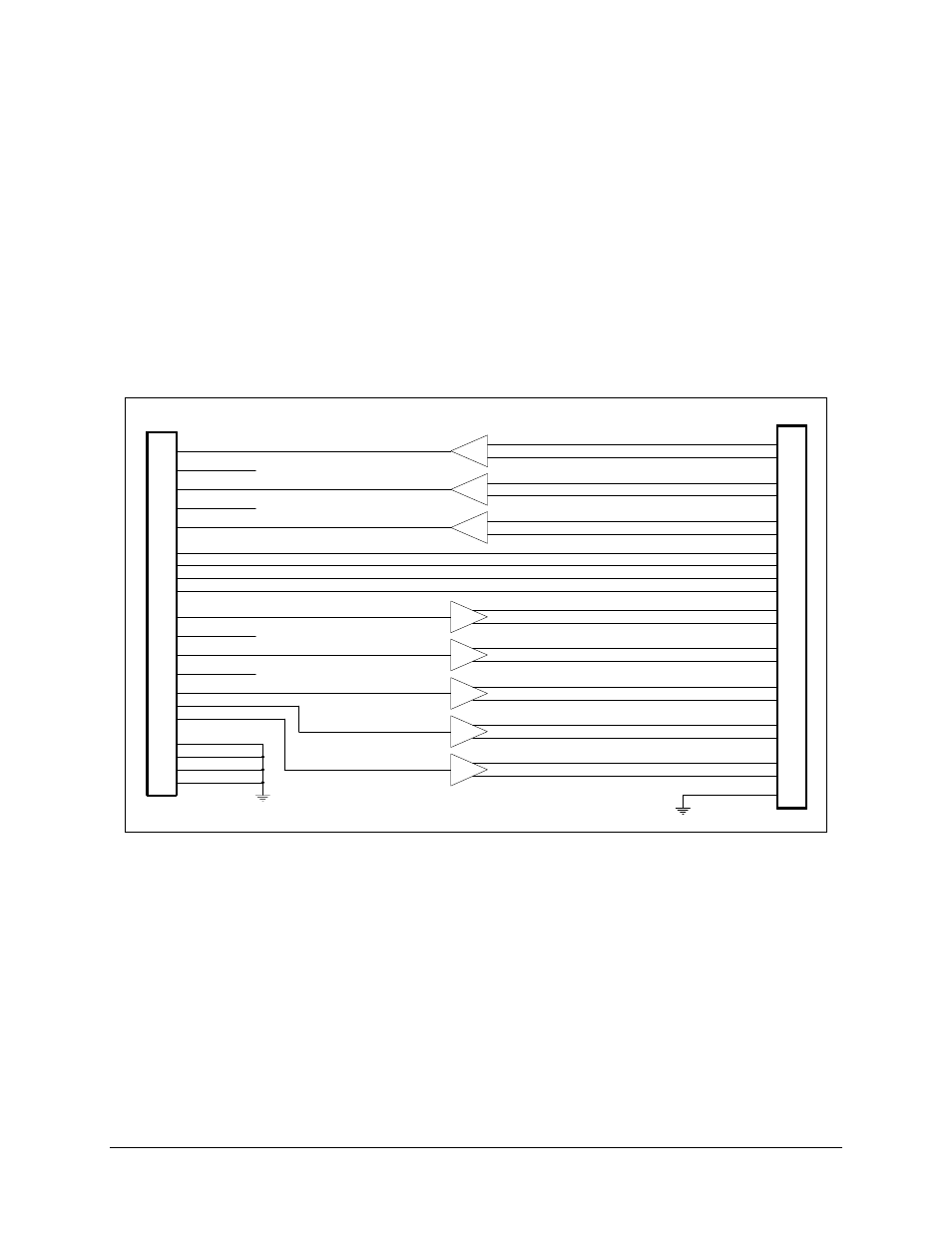
Figure 4-4. EIA-422/449 Diagram
Data received by the modem is output on the Received Data (RD) lines, while the
recovered clock is output on the Receive Timing (RT) lines.
For applications that require the rising edge of the clock to occur in the middle of the
data bit time, receive clock Normal mode should be selected.
Invert mode puts the falling edge of RT in the middle of the data bit. This selection can
be made from the front panel in the Configuration menu or from a remote terminal.