Table 6.6 capacitance, Table 6.7 output signals—inta/, intb, Capacitance – Avago Technologies LSI53C876E User Manual
Page 236: Output signals—inta/, intb
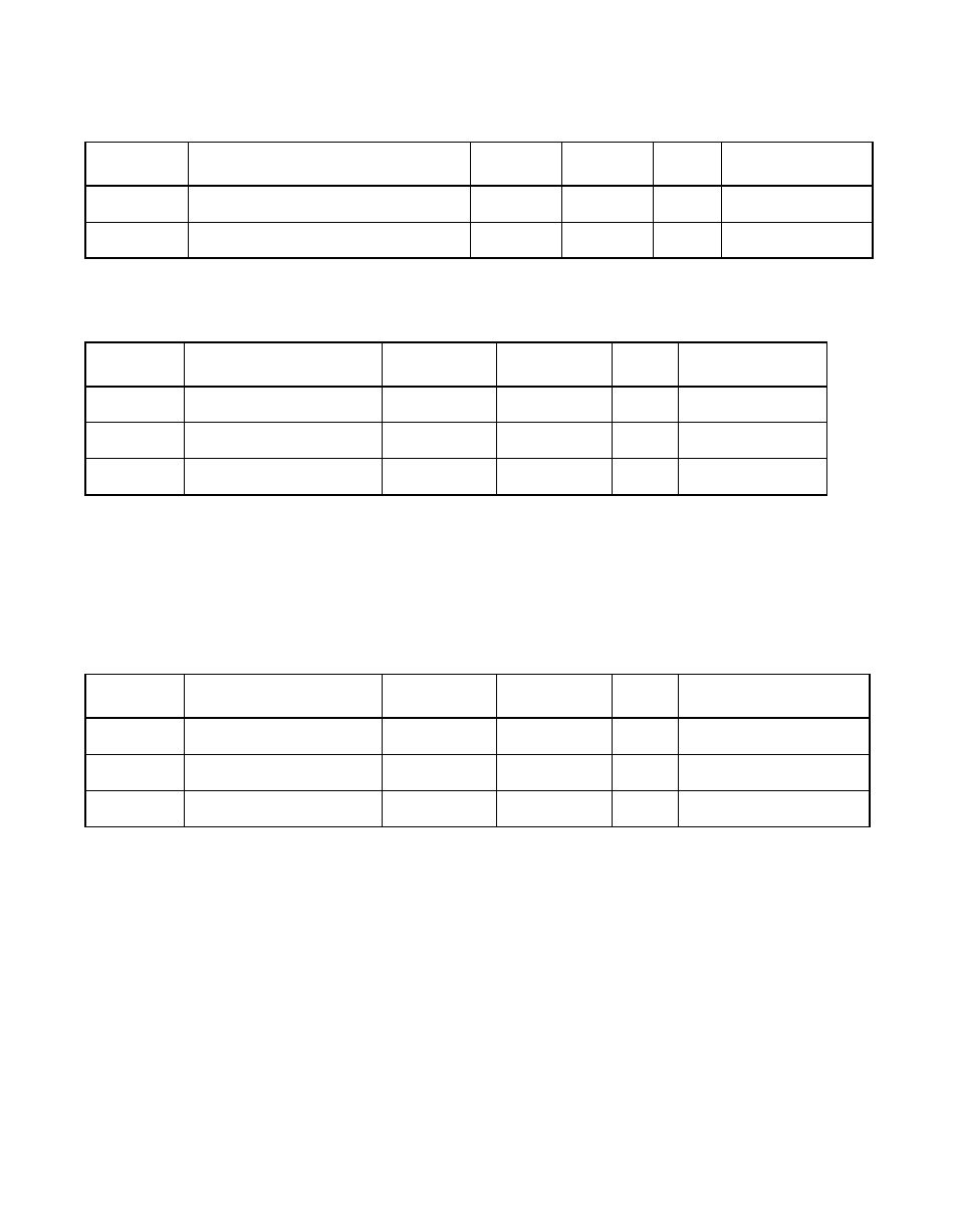
6-4
Electrical Characteristics
Table 6.6
Capacitance
Symbol
Parameter
Min
Max
Unit
Test Conditions
C
I
Input capacitance of input pads
–
7
pF
–
C
IO
Input capacitance of I/O pads
–
10
pF
–
Table 6.7
Output Signals—INTA/, INTB/
Symbol
Parameter
Min
Max
Unit
Test Conditions
V
OH
Output high voltage
2.4
V
DD
V
−
16 mA
V
OL
Output low voltage
V
SS
0.4
V
16 mA
I
OZ
3-state leakage
−
200
−
50
µ
A
–
Note: INTA/ and INTB/ have 100
µ
A pull-ups that are enabled when TESTIN is low. INTA/ and
INTB/ can be enabled with a register bit as an open drain output with an internal 100
µ
A
pull-up.
Table 6.8
Output Signals—SDIR[15:0], SDIRP0, SDIRP1, BSYDIR, SELDIR, RSTDIR,
TGS, IGS, MAS/[1:0], MCE/, MOE/_TESTOUT, MWE/
Symbol
Parameter
Min
Max
Unit
Test Conditions
V
OH
Output high voltage
2.4
V
DD
V
−
4 mA
V
OL
Output low voltage
V
SS
0.4
V
4 mA
I
OZ
3-state leakage
−
10
10
µ
A
–
Note: Each of these output signals have a 100
µ
A pull-up that is enabled when TESTIN is low.