Altera Nios Development Board User Manual
Page 14
2–6
Altera
Corporation
Nios Development Board Reference Manual, Stratix II Edition
July 2005
Component List
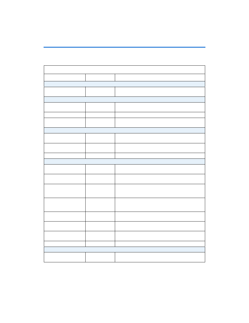
Table 2–1. Nios Development Board, Stratix Edition Components & Interfaces (Part 1 of 2)
Board Designation
Name
Description
Featured Device
U60
Stratix II FPGA
EP2S60F672C5 or EP2S30F672C5 device with mounted
heat sink
User Interface
SW0 – SW3
Push-button
switches
Four momentary contact switches for user input to the FPGA
D0 – D7
Individual LEDs
Eight individual LEDs driven by the FPGA
U8, U9
Seven-segment
LEDs
Two seven-segment LEDs to display numeric output from the
FPGA
Memory
U35, U36
SRAM memory
Two SRAM chips combined to form 1 Mbyte of fast, static
RAM
U5
Flash memory
16 Mbytes of nonvolatile memory for use by both the FPGA
and the configuration controller
U57
SDRAM memory
16 Mbytes of SDRAM
Connectors & Interfaces
U4, RJ1
Ethernet
MAC/PHY
10/100 Ethernet MAC/PHY chip connected to an RJ-45
Ethernet connector
J19, J27
Serial connectors
Two serial connectors with 5 V-tolerant buffers. Supports all
RS-232 signals.
PROTO1 (J11, J12, J13)
Expansion
prototype
connector
Expansion headers connecting to 41 I/O pins on the FPGA.
Supplies 3.3V and 5.0V for use by a daughter card.
PROTO2 (J15, J16, J17)
Expansion
prototype
connector
Expansion headers connecting to 41 I/O pins on the FPGA.
Supplies 3.3V and 5.0V for use by a daughter card.
CON3
CompactFlash
connector
CompactFlash connector for memory expansion
J25
Mictor connector
Mictor connector for debugging Nios II systems using a First
Silicon Solutions (FS2) debug probe.
J24
JTAG connector
Connects to the FPGA allowing hardware configuration from
Quartus II software and software debug from the Nios II IDE.
J5
JTAG connector
Connects to the configuration controller
Configuration & Reset
U3
Configuration
controller
Altera EPM7128AE device used to configure the FPGA from
flash memory