Altera Nios Development Board User Manual
Page 16
2–8
Altera
Corporation
Nios Development Board Reference Manual, Stratix II Edition
July 2005
Stratix II Device (U60)
The development board provides two separate methods for configuring
the Stratix II device:
1.
Using the Quartus II software running on a host computer, a
designer configures the device directly via an Altera
®
download
cable connected to the Stratix II JTAG header (J24).
2.
When power is applied to the board, a configuration controller
device (U3) attempts to configure the Stratix II device with
hardware configuration data stored in flash memory. For more
information on the configuration controller, see
Controller Device (U3)” on page 2–25
f
For Stratix II-related documentation including Stratix II pinout data refer
to the Altera Stratix II literature page at www.altera.com/ literature/lit-
stx2.html
.
Early shipments of the board had a heat sink mounted on the Stratix II
FPGA. Boards shipped later than May 2005 do not include the heat sink,
because thermal management is unnecessary for the majority of FPGA
designs for this board. A heat sink maintains the FPGA within its
specified thermal operating range, independent of the resource
utilization, clock frequency, and operating conditions of the FPGA. The
heat sink used on early shipments of the board is produced by Intricast
Inc., part number CS1995V01. See www.intricast.com for details.
f
Refer to Altera's AN185: Thermal Management Using Heat Sinks for
information on using heat sinks with Altera devices.
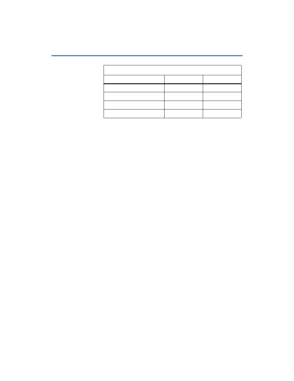
18-bit x 18-bit multipliers
64
144
Enhanced PLLS
2
4
Fast PLLs
4
8
User I/O pins
500
492
Table 2–2. Stratix II Device Features (Part 2 of 2)
Feature
EP2S30
EP2S60