Altera Nios Development Board User Manual
Page 27
Advertising
Altera Corporation
2–19
July 2005
Nios Development Board Reference Manual, Stratix II Edition
Board Components
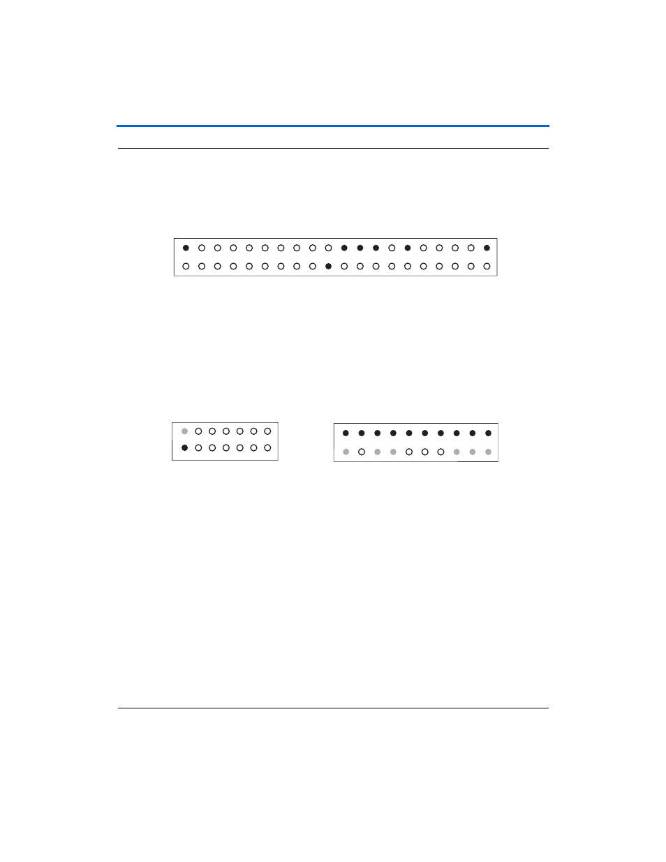
Figure 2–10. 6PROTO2 Pin Information - J15, J16 & J17
(1)
Unregulated voltage from DC power supply
(2)
Clk from board oscillator
(3)
Clk from FPGA via buffer
(4)
Clk output from protocard to FPGA
RESET_n
H15
C16
C17
F17
G17
C18
A20
A21
GND
C21
A22
E18
J18
C22
B22
B24
K17
J14
H18
GND
J15
A17
A18
K16
A19
C19
J17
C20
NC
GND
GND
GND
D18
GND
A24
NC
H17
B21
GND
1
3
5
7
9
11
13
15
17
19
21
23
25
27
29
31
33
35
37
39
2
4
6
8
10
12
14
16
18
20
22
24
26
28
30
32
34
36
38
40
J15
J16
(1)
V
u
nreg (U
5
4 pin 2)
N
C
V
C
C
3_3
V
C
C
3_3
(2)
P
RO
TO
2
_O
SC
(U
2 pin 6)
(3)
P
RO
TO
2
_C
LK
IN
(U
2 pin
17)
(4)
P
RO
TO
2
_C
LK
O
U
T (B
1
4)
V
C
C
3_3
V
C
C
3_3
V
C
C
3_3
G
N
D
G
N
D
G
N
D
G
N
D
G
N
D
G
N
D
G
N
D
G
N
D
G
N
D
G
N
D
1
3
5
7
9
11
13
15
17
19
2
4
6
8
10
12
14
16
18
20
G
N
D
B20
F16
D
17
B
16
B
18
E17
V
C
C
5
K
18
H
16
G
16
B17
B19
G
18
1
3
5
7
9
11
13
2
4
6
8
10
12
14
J17
Advertising