Scsi test one (stest1), Register: 0x4d (0xcd) – Avago Technologies LSI8751D User Manual
Page 188
5-72
SCSI Operating Registers
Register: 0x4D (0xCD)
SCSI Test One (STEST1)
Read/Write
SCLK
SCSI Clock
7
When set, this bit disables the external SCLK (SCSI
Clock) pin, and the chip uses the PCI clock as the
internal SCSI clock. If a transfer rate of 10 Mbytes/s (or
20 Mbytes/s on a wide SCSI bus) is desired on the SCSI
bus, this bit must be cleared and a 40 MHz external
SCLK must be provided.
SISO
SCSI Isolation Mode
6
This bit allows the LSI53C875 to put the SCSI
bidirectional and input pins into a low power mode when
the SCSI bus is not in use. When this bit is set, the SCSI
bus inputs are logically isolated from the SCSI bus.
R
Reserved
[5:4]
DBLEN
Doubler Enable
3
Set this bit to bring the SCSI clock doubler out of the
powered-down state. The default value of this bit is clear
(SCSI clock doubler powered down). Set bit 2 after
setting this bit, to double the SCLK frequency.
DBLSEL
Doubler Select
2
Set this bit after powering up the SCSI clock doubler to
double the SCLK frequency. This bit has no effect unless
bit 3 is set.
R
Reserved
[1:0]
5.0.0.1 Doubling the SCSI CLK Frequency
The LSI53C875 SCSI clock doubler doubles a 40 MHz SCSI clock,
increasing the frequency to 80 MHz. Follow these steps to use the clock
doubler:
1.
Set the SCLK Doubler Enable bit (
, bit 3).
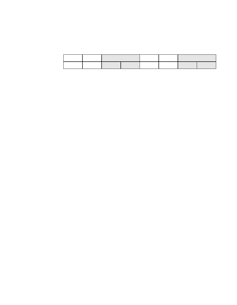
7
6
5
4
3
2
1
0
SCLK
SISO
R
DBLEN
DBLSEL
R
0
0
x
x
0
0
x
x