Avago Technologies LSI8751D User Manual
Page 274
Advertising
7-38
Instruction Set of the I/O Processor
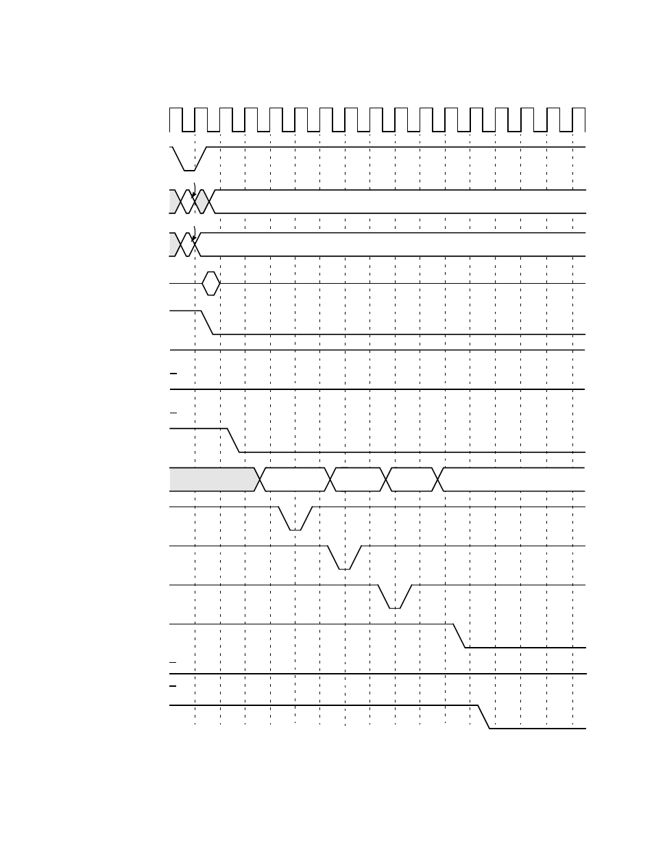
Figure 7.24 Write Cycle, Normal/Fast Memory (
≥
64 Kbyte), Multiple Byte Access
1
2
3
4
5
6
7
8
9
10
11
12
13
14
15
16
CLK
(Driven by System)
FRAME/
(Driven by Master)
AD
(Driven by Master-Addr;
C_BE/
(Driven by Master)
LSI53C875-Data)
PAR
(Driven by Master-Addr;
LSI53C875-Data)
IRDY/
(Driven by Master)
TRDY/
(Driven by LSI53C875)
STOP/
(Driven by LSI53C875)
DEVSEL/
(Driven by LSI53C875)
MAD
(Driven by LSI53C875)
GPIO2_MAS2/
(Driven by LSI53C875)
MAS1/
(Driven by LSI53C875)
MAS0/
(Driven by LSI53C875)
MOE/
(Driven by LSI53C875)
MCE/
(Driven by LSI53C875)
MWE/
(Driven by LSI53C875)
In
Addr
CMD
In
Byte Enable
High Order
Address
Middle Order
Address
Low Order
Address
Data In
Data Out
Advertising
This manual is related to the following products: