Serial data signals – Altera Arria V GZ Avalon-ST User Manual
Page 112
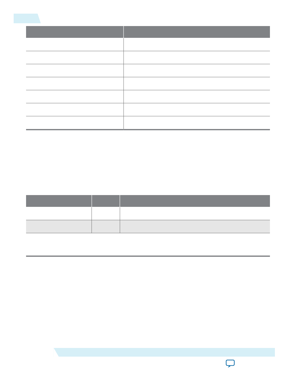
Variant
Logical Interfaces
Gen1 and Gen2 ×2
3
Gen1 and Gen2 ×4
5
Gen1 and Gen2 ×8
10
Gen3 ×1
3
Gen3 ×2
4
Gen3 ×4
6
Gen3 ×8
11
For more information about the Transceiver Reconfiguration Controller, refer to the Transceiver Reconfi‐
guration Controller chapter in the Altera Transceiver PHY IP Core User Guide .
Related Information
Serial Data Signals
Table 5-23: 1-Bit Interface Signals
Signal
Direction
Description
tx_out[7:0]
(1)
Output
Transmit output. These signals are the serial outputs of lanes 7–0.
rx_in[7:0]
(1)
Input
Receive input. These signals are the serial inputs of lanes 7–0.
Note:
1. The x1 IP core only has lane 0. The x2 IP core only has lanes 1–0. The x4 IP core only has lanes 3–0.
Refer to Pin-out Files for Altera Devices for pin-out tables for all Altera devices in .pdf, .txt, and .xls
formats.
Transceiver channels are arranged in groups of six. For GX devices, the lowest six channels on the left side
of the device are labeled GXB_L0, the next group is GXB_L1, and so on. Channels on the right side of the
device are labeled GXB_R0, GXB_R1, and so on. Be sure to connect the Hard IP for PCI Express on the
left side of the device to appropriate channels on the left side of the device, as specified in the Pin-out Files
for Altera Devices.
Related Information
5-60
Serial Data Signals
UG-01127_avst
2014.12.15
Altera Corporation
Interfaces and Signal Descriptions