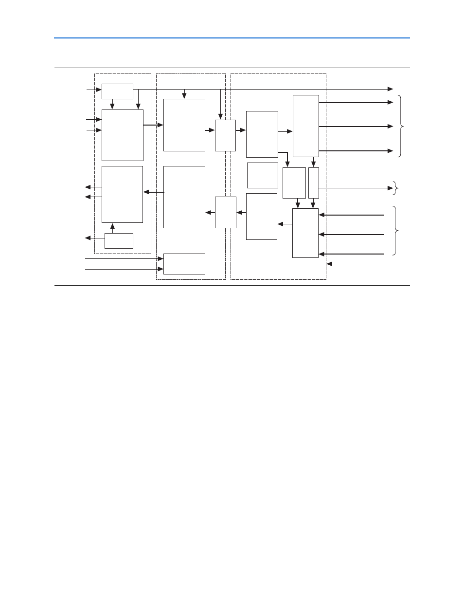
Physical interface, Synchronization and alignment, Figure 3–3 – Altera HyperTransport MegaCore Function User Manual
Page 30: Shows, Rx deserialization logic and clock generation, Tx serialization logic and clock generation
3–4
Chapter 3: Specifications
HyperTransport MegaCore Function Specification
HyperTransport MegaCore Function User Guide
© November 2009
Altera Corporation
Preliminary
Physical Interface
The physical interface module contains the logic that interfaces the HyperTransport
MegaCore function to the physical link signals. It contains the logic for both the
receiver and transmitter portions. The SERDES functionality is embedded into the
Altera device to ensure operation at maximum speed.
Rx Deserialization Logic and Clock Generation
This module receives serial data from each
RxCTL_i
and
RxCAD_i
bit and converts it
to a parallel data stream. The Rx clock generator (implemented in a fast PLL)
multiplies the receiver Rx link
RxClk_i
by two to capture
RxCTL_i
and
RxCAD_i
.
The data is then deserialized by a factor of eight and clocked by a divided-by-four
clock for use in the synchronization and alignment layer.
Tx Serialization Logic and Clock Generation
This module transmits serial data on the link interface. Data is transferred from the
internal module in parallel and is serialized on the link interface. The data entering
this module is already split into channels. The serialization circuit drives
TxCAD_o
and
TxCTL_o
. The Tx clock generator multiplies the Tx alignment logic clock by eight
to serialize the
TxCTL_o
and
TxCAD_o
signals, and generates a multiplied-by-four
clock for use as the HT
TxClk_o
.
Synchronization and Alignment
The synchronization and alignment layer is responsible for synchronizing clock
domains and aligning data to the natural boundaries.
Figure 3–3. HyperTransport MegaCore Function Block Diagram
TxPHY
Rx Alignment
Tx Alignment
Rx
Claimed
Buffers
Rx Packet
Processor
Tx Packet
Buffering
End-
Chain
Handler
Tx Packet
Scheduling
&
Framing
Protocol Interface
Synch & Alignment
Physical Interface
Reset Generation
RxPHY
Tx Clock
Generation
RxClk_i
RxCAD_i[7:0]
RxCTL_i
TxClk_o
TxCAD_o[7:0]
TxCTL_o
Rstn
PwrOk
C
S
R
Rx
Interface
Tx &Rx
Buffer Credit
Counters
CSR
Interface
Rx
Sync
FIFO
Tx
Interface
Tx
Sync
FIFO
Rx Response Req/Data
Rx Posted Req/Data
Rx Non-Posted Req/Data
Tx Response Req/Data
Tx Posted Req/Data
Tx Non-Posted Req/Data
Rx Clock
Generation
×
2
÷
4
Rx Link Clock Divided by 4
×
8
×
4
Ref Clk