Board overview, Board overview –2, Figure 2–1 – Altera Cyclone V E FPGA Development Board User Manual
Page 10: Table 2–1
2–2
Chapter 2: Board Components
Board Overview
Cyclone V E FPGA Development Board
March 2013
Altera Corporation
Reference Manual
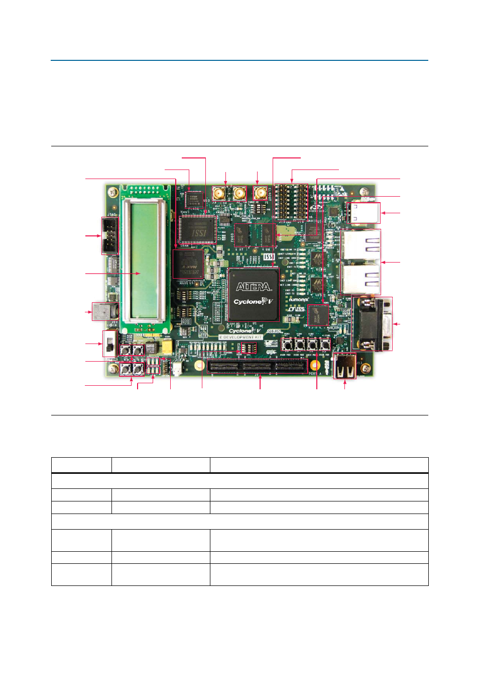
Board Overview
This section provides an overview of the Cyclone V E FPGA development board,
including an annotated board image and component descriptions.
shows
an overview of the board features.
describes the components and lists their corresponding board references.
Figure 2–1. Overview of the Cyclone V E FPGA Development Board Features
Clock Input SMA
Connectors
(J2, J3)
General User
Push Buttons
(S5-S8)
Flash x16 Memory (U10)
LPDDR2 x16
Memory (U9)
Serial UART
Connector
(J12)
DDR3 x32
Memory
(U7, U8)
DC Input
Jack (J17)
Character
LCD (J14)
CPU Reset,
MAX V Reset
Push Buttons
(S3, S4)
Power Switch
(SW5)
User
DIP Switch
(SW3)
MAX V CPLD
EPM2210 System
Controller (U13)
Clock Output
SMA Connector
(J4)
HSMC Port
(J1)
Configuration Done,
Load, and Error
LEDs (D17-D19)
Program Config,
Program Select
Push Buttons
(S1, S2)
Program Select
LEDs (D25-D27)
USB Type-B
Connector
(J10)
USB-UART
Connector (J13)
SSRAM x16 Memory (U11)
Debug Headers (J15, J16)
Gigabit
Ethernet
Port (J11)
JTAG Chain
Header
(J4)
Cyclone V E FPGA (U1)
Table 2–1. Board Components (Part 1 of 3)
Board Reference
Type
Description
Featured Devices
U1
FPGA
Cyclone V E FPGA, 5CEFA7F31I7N, 896-pin FBGA.
U13
CPLD
MAX V CPLD, 5M2210ZF256I5N, 256-pin FBGA.
Configuration, Status, and Setup Elements
J4
JTAG chain header
Provides access to the JTAG chain and disables the embedded
USB-Blaster II when using an external USB-Blaster cable.
SW2
JTAG chain control DIP switch Remove or include devices in the active JTAG chain.
J10
USB type-B connector
USB interface for FPGA programming and debugging through the
embedded USB-Blaster II JTAG via a type-B USB cable.