Components and interfaces, 10/100/1000 ethernet, Components and interfaces –24 – Altera Cyclone V E FPGA Development Board User Manual
Page 32: 10/100/1000 ethernet –24
2–24
Chapter 2: Board Components
Components and Interfaces
Cyclone V E FPGA Development Board
March 2013
Altera Corporation
Reference Manual
Components and Interfaces
This section describes the development board's communication ports and interface
cards relative to the Cyclone V E FPGA device. The development board supports the
following communication ports:
■
RS-232 Serial UART
■
10/100/1000 Ethernet
■
HSMC
■
USB UART
10/100/1000 Ethernet
The development board supports two 10/100/1000 base-T Ethernet using two
external Marvell 88E1111 PHY and Altera Triple-Speed Ethernet MegaCore MAC
function. The PHY-to-MAC interfaces employ RGMII interface. The MAC function
must be provided in the FPGA for typical networking applications.
The Marvell 88E1111 PHY uses 2.5-V and 1.0-V power rails and requires a 25-MHz
reference clock driven from a dedicated oscillator. The PHY interfaces to a RJ45 model
with internal magnetics that can be used for driving copper lines with Ethernet traffic.
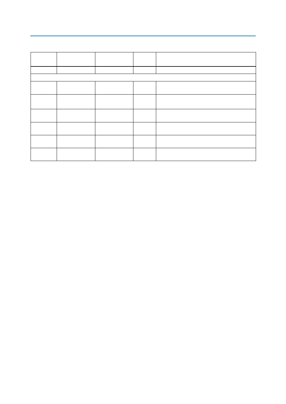
16
HEADER_D7
B27
1.5-V
Single-ended signal for debug purposes only
Debug Header (J16)
1 and 2
HEADER_P0 and
HEADER_N0
H25 and H26
2.5-V
Pseudo-differential signals for debug purposes only
3 and 4
HEADER_P1 and
HEADER_N1
P20 and N20
2.5-V
Pseudo-differential signals for debug purposes only
7 and 8
HEADER_P2 and
HEADER_N2
J22 and J23
2.5-V
Pseudo-differential signals for debug purposes only
9 and 10
HEADER_P3 and
HEADER_N3
D28 and D29
2.5-V
Pseudo-differential signals for debug purposes only
13 and 14
HEADER_P4 and
HEADER_N4
E27 and D27
2.5-V
Pseudo-differential signals for debug purposes only
15 and 16
HEADER_P5 and
HEADER_N5
H24 and J25
2.5-V
Pseudo-differential signals for debug purposes only
Table 2–19. Debug Header Pin Assignments, Schematic Signal Names, and Functions (Part 2 of 2)
Board
Reference
Schematic Signal
Name
Cyclone V E FPGA
Pin Number
I/O
Standard
Description