Flash, Flash –39 – Altera Cyclone V E FPGA Development Board User Manual
Page 47
Chapter 2: Board Components
2–39
Memory
March 2013
Altera Corporation
Cyclone V E FPGA Development Board
Reference Manual
Flash
The development board supports a 512-Mb CFI-compatible synchronous flash device
for non-volatile storage of FPGA configuration data, board information, test
application data, and user code space. This device is part of the shared FSM bus that
connects to the flash memory, SSRAM, and MAX V CPLD 5M2210 System Controller.
This 16-bit data memory interface can sustain burst read operations at up to 52 MHz
for a throughput of 832 Mbps per device. The write performance is 270 µs for a single
word buffer while the erase time is 800 ms for a 128 K array block.
lists the flash pin assignments, signal names, and functions. The signal
names and types are relative to the Cyclone V E FPGA in terms of I/O setting and
direction.
72
FSM_D6
E12
2.5-V
Data bus
73
FSM_D7
D13
2.5-V
Data bus
23
FSM_D8
J15
2.5-V
Data bus
22
FSM_D9
H15
2.5-V
Data bus
19
FSM_D10
E11
2.5-V
Data bus
18
FSM_D11
D10
2.5-V
Data bus
12
FSM_D12
L10
2.5-V
Data bus
13
FSM_D13
L9
2.5-V
Data bus
8
FSM_D14
G14
2.5-V
Data bus
9
FSM_D15
F14
2.5-V
Data bus
85
SRAM_ADSCN
E6
2.5-V
Address status controller
84
SRAM_ADSPN
J10
2.5-V
Address status processor
83
SRAM_ADVN
G6
2.5-V
Address valid
93
SRAM_BWAN
A3
2.5-V
Byte write select
94
SRAM_BWBN
A2
2.5-V
Byte write select
97
SRAM_CE2
—
2.5-V
Chip enable 2
92
SRAM_CE3N
—
2.5-V
Chip enable 3
98
SRAM_CEN
D7
2.5-V
Chip enable 1
89
SRAM_CLK
K10
2.5-V
Clock
88
SRAM_GWN
—
2.5-V
Global write enable
31
SRAM_MODE
—
2.5-V
Burst sequence selection
64
SRAM_ZZ
—
2.5-V
Power sleep mode
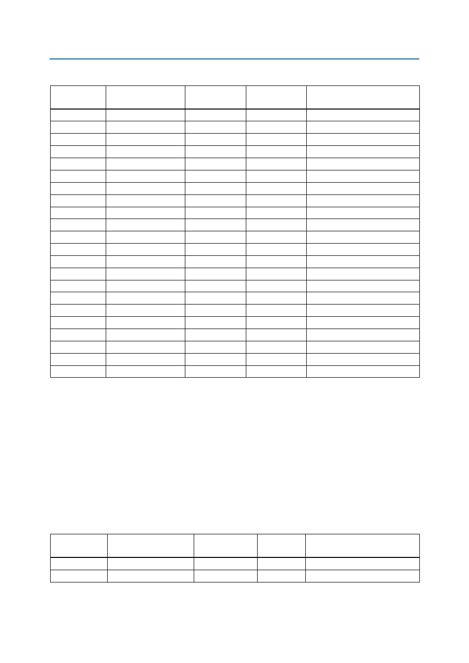
Table 2–27. SSRAM Pin Assignments, Schematic Signal Names, and Functions (Part 2 of 2)
Board
Reference (U11)
Schematic
Signal Name
Cyclone V E FPGA
Pin Number
I/O Standard
Description
Table 2–28. Flash Pin Assignments, Schematic Signal Names, and Functions (Part 1 of 3)
Board
Reference (U10)
Schematic Signal Name
Cyclone V E FPGA
Pin Number
I/O Standard
Description
F6
FLASH_ADVN
H12
2.5-V
Address valid
B4
FLASH_CEN
H14
2.5-V
Chip enable