Altera Cyclone V E FPGA Development Board User Manual
Page 17
Chapter 2: Board Components
2–9
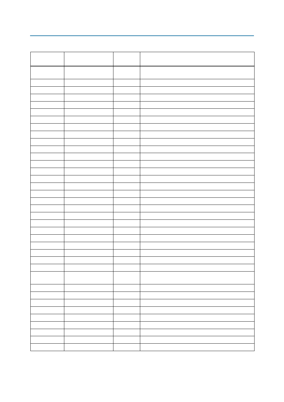
MAX V CPLD 5M2210 System Controller
March 2013
Altera Corporation
Cyclone V E FPGA Development Board
Reference Manual
P11
M570_CLOCK
2.5-V
25-MHz clock to embedded USB-Blaster II for sending
FACTORY command
M1
M570_JTAG_EN
3.3-V
Low signal to disable the embedded USB-Blaster II
P10
MAX5_BEN0
2.5-V
FSM bus MAX V byte enable 0
R11
MAX5_BEN1
2.5-V
FSM bus MAX V byte enable 1
T12
MAX5_BEN2
2.5-V
FSM bus MAX V byte enable 2
N11
MAX5_BEN3
2.5-V
FSM bus MAX V byte enable 3
T11
MAX5_CLK
2.5-V
FSM bus MAX V clock
R10
MAX5_CSN
2.5-V
FSM bus MAX V chip select
M10
MAX5_OEN
2.5-V
FSM bus MAX V output enable
N10
MAX5_WEN
2.5-V
FSM bus MAX V write enable
E11
MAX_CONF_DONEN
2.5-V
Embedded USB-Blaster II configuration done LED
A4
MAX_ERROR
2.5-V
FPGA configuration error LED
A6
MAX_LOAD
2.5-V
FPGA configuration active LED
M9
MAX_RESETN
2.5-V
MAX V reset push button
B7
OVERTEMP
2.5-V
Temperature monitor fan enable
D12
PGM_CONFIG
2.5-V
Load the flash memory image identified by the PGM LEDs
B14
PGM_LED0
2.5-V
Flash memory PGM select indicator 0
C13
PGM_LED1
2.5-V
Flash memory PGM select indicator 1
B16
PGM_LED2
2.5-V
Flash memory PGM select indicator 2
B13
PGM_SEL
2.5-V
Toggles the PGM_LED[2:0] LED sequence
H4
PSAS_CSn
3.3-V
AS configuration chip select
G1
PSAS_DCLK
3.3-V
AS configuration clock
G4
PSAS_CONF_DONE
3.3-V
AS configuration done
H2
PSAS_CONFIGn
3.3-V
AS configuration active
G5
PSAS_DATA1
3.3-V
AS configuration data
H3
PSAS_DATA0_ASD0
3.3-V
AS configuration data
J1
PSAS_CEn
3.3-V
AS configuration chip enable
R12
SECURITY_MODE
2.5-V
DIP switch for the embedded USB-Blaster II to send FACTORY
command at power up
E7
SENSE_CS0N
2.5-V
Power monitor chip select
A5
SENSE_SCK
2.5-V
Power monitor SPI clock
D7
SENSE_SDI
2.5-V
Power monitor SPI data in
B6
SENSE_SDO
2.5-V
Power monitor SPI data out
A9
SI570_EN
2.5-V
Si570 programmable XO enable
R4
USB_CFG0
2.5-V
Embedded USB-Blaster II interface. Reserved for future use
T4
USB_CFG1
2.5-V
Embedded USB-Blaster II interface. Reserved for future use
P8
USB_CFG2
2.5-V
Embedded USB-Blaster II interface. Reserved for future use
T7
USB_CFG3
2.5-V
Embedded USB-Blaster II interface. Reserved for future use
Table 2–4. MAX V CPLD 5M2210 System Controller Device Pin-Out (Part 4 of 5)
Board
Reference (U13)
Schematic Signal Name
I/O Standard
Description