Altera Cyclone V E FPGA Development Board User Manual
Page 36
2–28
Chapter 2: Board Components
Components and Interfaces
Cyclone V E FPGA Development Board
March 2013
Altera Corporation
Reference Manual
The HSMC interface has programmable bi-directional I/O pins that can be used as
2.5-V LVCMOS, which is 3.3-V LVTTL-compatible. These pins can also be used as
various differential I/O standards including, but not limited to, LVDS, mini-LVDS,
and RSDS with up to 17 full-duplex channels.
1
As noted in the
manual, LVDS and
single-ended I/O standards are only guaranteed to function when mixed according to
either the generic single-ended pin-out or generic differential pin-out.
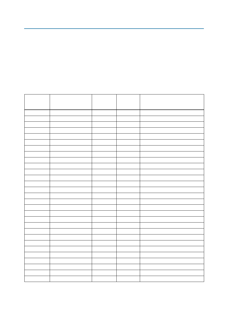
Table 2–21
lists the HSMC interface pin assignments, signal names, and functions.
Table 2–21. HSMC Interface Pin Assignments, Schematic Signal Names, and Functions (Part 1 of 3)
Board
Reference (J7)
Schematic Signal Name
Cyclone V E
FPGA Pin
Number
I/O Standard
Description
33
HSMC_SDA
AB22
2.5-V CMOS
Management serial data
34
HSMC_SCL
AC22
2.5-V CMOS
Management serial clock
35
JTAG_TCK
AC7
2.5-V CMOS
JTAG clock signal
36
HSMC_JTAG_TMS
—
2.5-V CMOS
JTAG mode select signal
37
HSMC_JTAG_TDO
—
2.5-V CMOS
JTAG data output
38
JTAC_FPGA_TDO_RETIMER
—
2.5-V CMOS
JTAG data input
39
HSMC_CLK_OUT0
AJ14
2.5-V CMOS
Dedicated CMOS clock out
40
HSMC_CLK_IN0
AB16
2.5-V CMOS
Dedicated CMOS clock in
41
HSMC_D0
AH10
2.5-V CMOS
Dedicated CMOS I/O bit 0
42
HSMC_D1
AJ10
2.5-V CMOS
Dedicated CMOS I/O bit 1
43
HSMC_D2
Y13
2.5-V CMOS
Dedicated CMOS I/O bit 2
44
HSMC_D3
AA14
2.5-V CMOS
Dedicated CMOS I/O bit 3
47
HSMC_TX_D_P0
AK27
LVDS or 2.5-V LVDS TX bit 0 or CMOS bit 4
48
HSMC_RX_D_P0
Y16
LVDS or 2.5-V LVDS RX bit 0 or CMOS bit 5
49
HSMC_TX_D_N0
AK28
LVDS or 2.5-V LVDS TX bit 0n or CMOS bit 6
50
HSMC_RX_D_N0
AA26
LVDS or 2.5-V LVDS RX bit 0n or CMOS bit 7
53
HSMC_TX_D_P1
AJ27
LVDS or 2.5-V LVDS TX bit 1 or CMOS bit 8
54
HSMC_RX_D_P1
Y17
LVDS or 2.5-V LVDS RX bit 1 or CMOS bit 9
55
HSMC_TX_D_N1
AK26
LVDS or 2.5-V LVDS TX bit 1n or CMOS bit 10
56
HSMC_RX_D_N1
Y18
LVDS or 2.5-V LVDS RX bit 1n or CMOS bit 11
59
HSMC_TX_D_P2
AG26
LVDS or 2.5-V LVDS TX bit 2 or CMOS bit 12
60
HSMC_RX_D_P2
AA18
LVDS or 2.5-V LVDS RX bit 2 or CMOS bit 13
61
HSMC_TX_D_N2
AH26
LVDS or 2.5-V LVDS TX bit 2n or CMOS bit 14
62
HSMC_RX_D_N2
AA19
LVDS or 2.5-V LVDS RX bit 2n or CMOS bit 15
65
HSMC_TX_D_P3
AJ25
LVDS or 2.5-V LVDS TX bit 3 or CMOS bit 16
66
HSMC_RX_D_P3
Y20
LVDS or 2.5-V LVDS RX bit 3 or CMOS bit 17
67
HSMC_TX_D_N3
AK25
LVDS or 2.5-V LVDS TX bit 3n or CMOS bit 18
68
HSMC_RX_D_N3
AA20
LVDS or 2.5-V LVDS RX bit 3n or CMOS bit 19
71
HSMC_TX_D_P4
AH24
LVDS or 2.5-V LVDS TX bit 4 or CMOS bit 20