Altera Cyclone V E FPGA Development Board User Manual
Page 14
2–6
Chapter 2: Board Components
MAX V CPLD 5M2210 System Controller
Cyclone V E FPGA Development Board
March 2013
Altera Corporation
Reference Manual
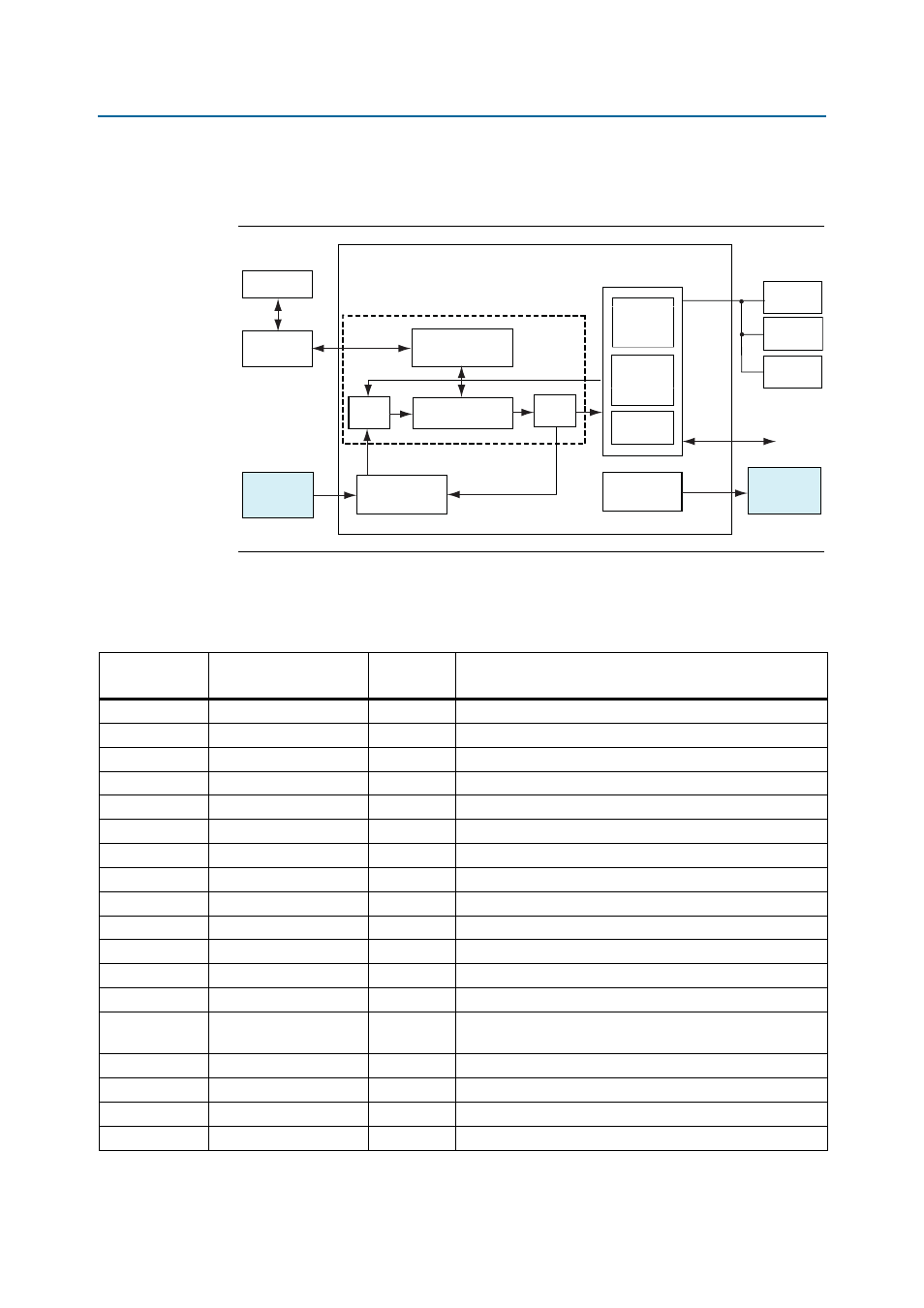
illustrates the MAX V CPLD 5M2210 System Controller's functionality and
external circuit connections as a block diagram.
lists the I/O signals present on the MAX V CPLD 5M2210 System
Controller. The signal names and functions are relative to the MAX V device.
Figure 2–2. MAX V CPLD 5M2210 System Controller Block Diagram
Information
Register
Embedded
USB-Blaster II
Si570
Controller
SLD-HUB
PFL
FSM Bus
MAX V CPLD System Controller
Power
Measurement
Results
Virtual-JTAG
PC
FPGA
LTC2418
Controller
Flash
Decoder
Encoder
GPIO
JTAG Control
SSRAM
Control
Register
Si570
Programmable
Oscillator
Table 2–4. MAX V CPLD 5M2210 System Controller Device Pin-Out (Part 1 of 5)
Board
Reference (U13)
Schematic Signal Name
I/O Standard
Description
N4
5M2210_JTAG_TMS
3.3-V
MAX V JTAG TMS
E9
CLK50_EN
2.5-V
50 MHz oscillator enable
H12
CLK_CONFIG
2.5-V
100 MHz configuration clock input
A15
CLK_ENABLE
2.5-V
DIP switch for clock oscillator enable
A13
CLK_SEL
2.5-V
DIP switch for clock select—SMA or oscillator
J12
CLKIN_50_MAXV
2.5-V
50 MHz clock input
D9
CLOCK_SCL
2.5-V
Programmable oscillator I
2
C clock
C9
CLOCK_SDA
2.5-V
Programmable oscillator I
2
C data
D10
CPU_RESETN
2.5-V
FPGA reset push button
P12
EXTRA_SIG0
2.5-V
Embedded USB-Blaster II interface. Reserved for future use
T13
EXTRA_SIG1
2.5-V
Embedded USB-Blaster II interface. Reserved for future use
T15
EXTRA_SIG2
2.5-V
Embedded USB-Blaster II interface. Reserved for future use
A2
FACTORY_LOAD
2.5-V
DIP switch to load factory or user design at power-up
R14
FACTORY_REQUEST
2.5-V
Embedded USB-Blaster II request to send FACTORY
command
N12
FACTORY_STATUS
2.5-V
Embedded USB-Blaster II FACTORY command status
C8
FAN_FORCE_ON
2.5-V
DIP switch to on or off the fan
N7
FLASH_ADVN
2.5-V
FSM bus flash memory address valid
R5
FLASH_CEN
2.5-V
FSM bus flash memory chip enable