Rs-232 serial uart, Rs-232 serial uart –30 – Altera Cyclone V E FPGA Development Board User Manual
Page 38
2–30
Chapter 2: Board Components
Components and Interfaces
Cyclone V E FPGA Development Board
March 2013
Altera Corporation
Reference Manual
RS-232 Serial UART
A female angled DSUB 9-pin connector along with a supporting RS-232 transceiver
provides support for implementing a standard RS-232 serial UART channel on this
board. The connector has the same pinouts as a data terminal device and requires only
a standard cable (no null modem required for PC interface). A dedicated level-shifting
buffer is used to translate between LVTTL and RS-232 levels. Board references D23
and D24 are serial UART LEDs that illuminate to indicate RX and TX activity.
lists the RS-232 serial UART pin assignments, signal names, and functions.
The signal names and types are relative to the Cyclone V E FPGA in terms of I/O
setting and direction.
128
HSMC_RX_D_N12
AK17
LVDS or 2.5-V LVDS RX bit 12n or CMOS bit 59
131
HSMC_TX_D_P13
AG17
LVDS or 2.5-V LVDS TX bit 13 or CMOS bit 60
132
HSMC_RX_D_P13
AF16
LVDS or 2.5-V LVDS RX bit 13 or CMOS bit 61
133
HSMC_TX_D_N13
AH17
LVDS or 2.5-V LVDS TX bit 13n or CMOS bit 62
134
HSMC_RX_D_N13
AG16
LVDS or 2.5-V LVDS RX bit 13n or CMOS bit 63
137
HSMC_TX_D_P14
AJ15
LVDS or 2.5-V LVDS TX bit 14 or CMOS bit 64
138
HSMC_RX_D_P14
AE16
LVDS or 2.5-V LVDS RX bit 14 or CMOS bit 65
139
HSMC_TX_D_N14
AK15
LVDS or 2.5-V LVDS TX bit 14n or CMOS bit 66
140
HSMC_RX_D_N14
AF15
LVDS or 2.5-V LVDS RX bit 14n or CMOS bit 67
143
HSMC_TX_D_P15
AH14
LVDS or 2.5-V LVDS TX bit 15 or CMOS bit 68
144
HSMC_RX_D_P15
AD17
LVDS or 2.5-V LVDS RX bit 15 or CMOS bit 69
145
HSMC_TX_D_N15
AH15
LVDS or 2.5-V LVDS TX bit 15n or CMOS bit 70
146
HSMC_RX_D_N15
AE17
LVDS or 2.5-V LVDS RX bit 15n or CMOS bit 71
149
HSMC_TX_D_P16
AE15
LVDS or 2.5-V LVDS TX bit 16 or CMOS bit 72
150
HSMC_RX_D_P16
AD18
LVDS or 2.5-V LVDS RX bit 16 or CMOS bit 73
151
HSMC_TX_D_N16
AF14
LVDS or 2.5-V LVDS TX bit 16n or CMOS bit 74
152
HSMC_RX_D_N16
AE18
LVDS or 2.5-V LVDS RX bit 16n or CMOS bit 75
155
HSMC_CLK_OUT_P2
AG23
LVDS or 2.5-V LVDS or CMOS clock out 2 or CMOS bit 76
156
HSMC_CLK_IN_P2
Y15
LVDS or 2.5-V LVDS or CMOS clock in 2 or CMOS bit 77
157
HSMC_CLK_OUT_N2
AH22
LVDS or 2.5-V LVDS or CMOS clock out 2 or CMOS bit 78
158
HSMC_CLK_IN_N2
AA15
LVDS or 2.5-V LVDS or CMOS clock in 2 or CMOS bit 79
160
HSMC_PRSNTn
AK5
2.5-V CMOS
HSMC port presence detect
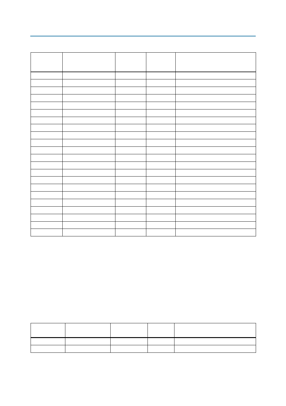
Table 2–21. HSMC Interface Pin Assignments, Schematic Signal Names, and Functions (Part 3 of 3)
Board
Reference (J7)
Schematic Signal Name
Cyclone V E
FPGA Pin
Number
I/O Standard
Description
Table 2–22. RS-232 Serial UART Schematic Signal Names and Functions
Board
Reference (U20)
Schematic
Signal Name
Cyclone V E FPGA
Pin Number
I/O Standard
Description
14
UART_TXD
AB9
3.3-V
Transmit data
15
UART_RTS
AH6
3.3-V
Request to send