Altera Cyclone V E FPGA Development Board User Manual
Page 15
Chapter 2: Board Components
2–7
MAX V CPLD 5M2210 System Controller
March 2013
Altera Corporation
Cyclone V E FPGA Development Board
Reference Manual
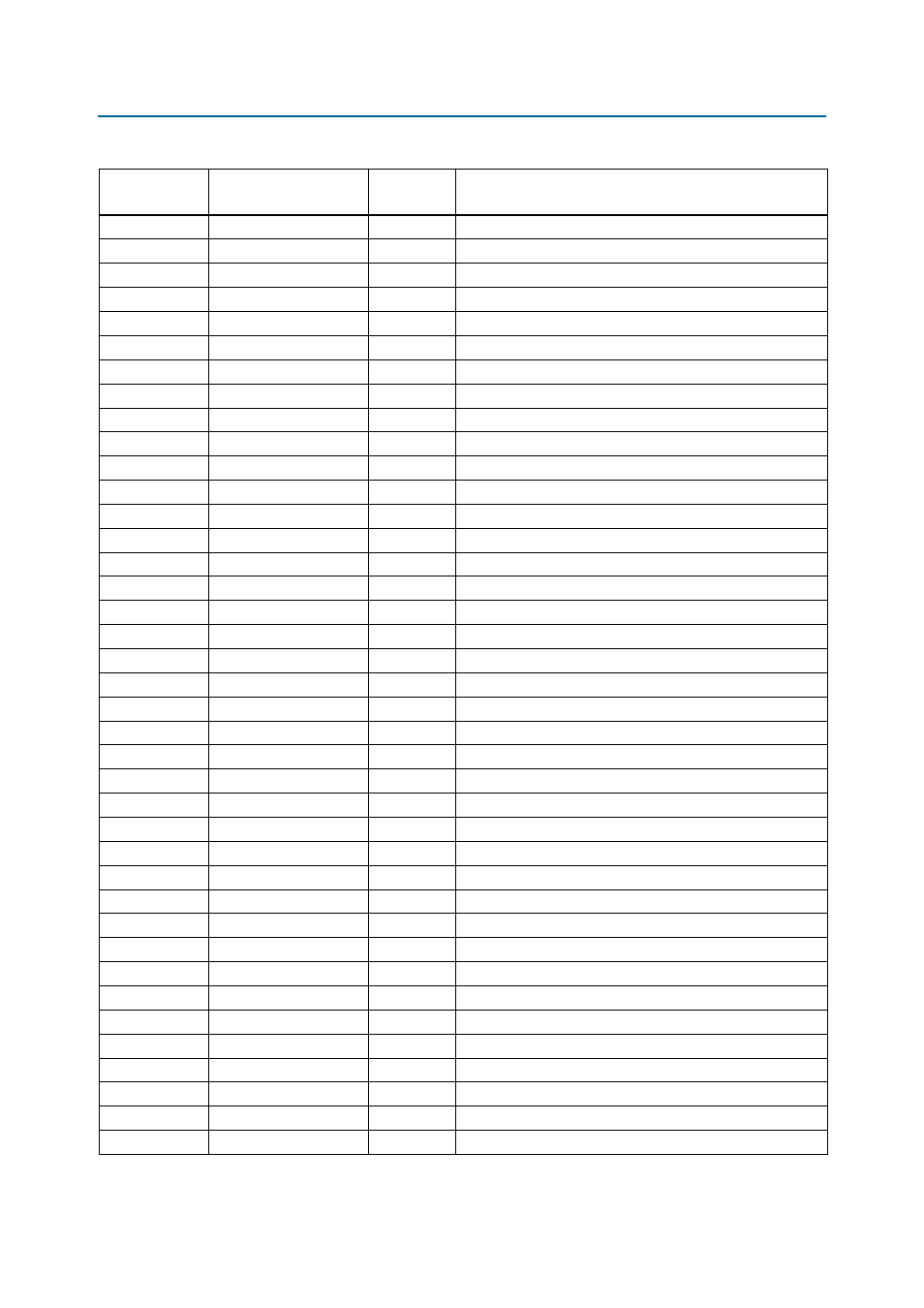
R6
FLASH_CLK
2.5-V
FSM bus flash memory clock
M6
FLASH_OEN
2.5-V
FSM bus flash memory output enable
T5
FLASH_RDYBSYN
2.5-V
FSM bus flash memory ready
P7
FLASH_RESETN
2.5-V
FSM bus flash memory reset
N6
FLASH_WEN
2.5-V
FSM bus flash memory write enable
K1
FPGA_CONF_DONE
3.3-V
FPGA configuration done LED
D3
FPGA_CONFIG_D0
3.3-V
FPGA configuration data
C2
FPGA_CONFIG_D1
3.3-V
FPGA configuration data
C3
FPGA_CONFIG_D2
3.3-V
FPGA configuration data
E3
FPGA_CONFIG_D3
3.3-V
FPGA configuration data
D2
FPGA_CONFIG_D4
3.3-V
FPGA configuration data
E4
FPGA_CONFIG_D5
3.3-V
FPGA configuration data
D1
FPGA_CONFIG_D6
3.3-V
FPGA configuration data
E5
FPGA_CONFIG_D7
3.3-V
FPGA configuration data
F3
FPGA_CONFIG_D8
3.3-V
FPGA configuration data
E1
FPGA_CONFIG_D9
3.3-V
FPGA configuration data
F4
FPGA_CONFIG_D10
3.3-V
FPGA configuration data
F2
FPGA_CONFIG_D11
3.3-V
FPGA configuration data
F1
FPGA_CONFIG_D12
3.3-V
FPGA configuration data
F6
FPGA_CONFIG_D13
3.3-V
FPGA configuration data
G2
FPGA_CONFIG_D14
3.3-V
FPGA configuration data
G3
FPGA_CONFIG_D15
3.3-V
FPGA configuration data
K4
FPGA_MAX_DCLK
3.3-V
FPGA configuration clock
J3
FPGA_DCLK
3.3-V
FPGA configuration clock
N1
FPGA_NCONFIG
3.3-V
FPGA configuration active
J4
FPGA_NSTATUS
3.3-V
FPGA configuration ready
H1
FPGA_PR_DONE
3.3-V
FPGA partial reconfiguration done
P2
FPGA_PR_ERROR
3.3-V
FPGA partial reconfiguration error
E2
FPGA_PR_READY
3.3-V
FPGA partial reconfiguration ready
F5
FPGA_PR_REQUEST
3.3-V
FPGA partial reconfiguration request
L5
FPGA_MAX_NCS
3.3-V
FPGA configuration chip select
E14
FSM_A1
2.5-V
FSM address bus
C14
FSM_A2
2.5-V
FSM address bus
C15
FSM_A3
2.5-V
FSM address bus
E13
FSM_A4
2.5-V
FSM address bus
E12
FSM_A5
2.5-V
FSM address bus
D15
FSM_A6
2.5-V
FSM address bus
F14
FSM_A7
2.5-V
FSM address bus
D16
FSM_A8
2.5-V
FSM address bus
Table 2–4. MAX V CPLD 5M2210 System Controller Device Pin-Out (Part 2 of 5)
Board
Reference (U13)
Schematic Signal Name
I/O Standard
Description