Altera Cyclone V E FPGA Development Board User Manual
Page 27
Chapter 2: Board Components
2–19
Clock Circuitry
March 2013
Altera Corporation
Cyclone V E FPGA Development Board
Reference Manual
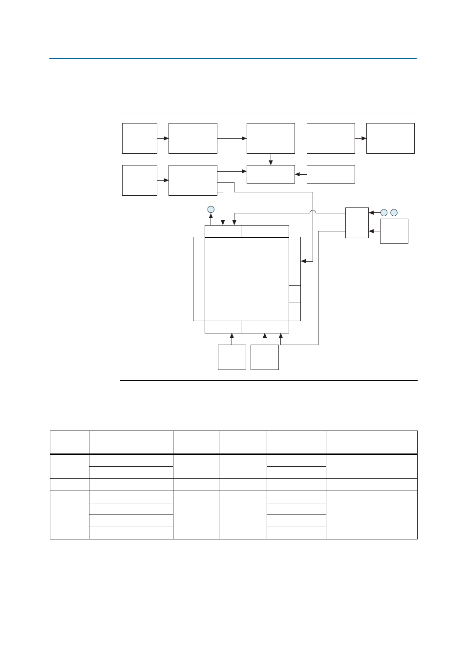
shows the default frequencies of all external clocks going to the
Cyclone V E FPGA development board.
Table 2–10
lists the oscillators, its I/O standard, and voltages required for the
development board.
Figure 2–6. Cyclone V E FPGA Development Board Clocks
FA-128
24.0000 MB-W
24 MHz
Crystal
Cypress
CY7C68013A
USB Microcontroller
MAX II
Embedded
USB-Blaster
Si510
SE 50 MHz
Fixed Oscillator
SL18860DC
Clock Fanout
X4 SE 50 MHz
Ch3
Ch2
Ch1
CLK_USB
48 MHz
SG-310DF
25.0000M-B3
25 MHz
Fixed Oscillator
10/100/1000
Base-T
Ethernet PHY
88E1111
Bank 8A
Bank 7A
Bank 3A Bank 3B
Bank 4A
Bank 5A
Bank 5B
Bank 6A
Tr
ansceiv
er Bloc
k
SMA Clock Out
Two Channels
Unused
Top Bank
Bottom Bank
SMA LVDS
Clock Input
Si570 LVDS
Clock Output
125 MHz
Programmable
LVDS
HSMC
Differential
Clock In x 2
HSMC SE
Clock In
MAX V CPLD 5M2210
System Controller
SI510 SE 100 MHz
Fixed Oscillator
ICS8543
Clock
Fanout
Table 2–10. On-Board Oscillators
Source
Schematic Signal Name
Frequency
I/O Standard
Cyclone V E
FPGA Pin Number
Application
U4
CLKIN_50_FPGA_TOP
50.000 MHz
Single-Ended
L14
Top and right edge
CLKIN_50_FPGA_RIGHT
P22
X3
CLK_CONFIG
100.000 MHz
2.5V CMOS
—
Fast FPGA configuration
X1 and U3
(buffer)
DIFF_CLKIN_TOP_125_P
125.000 MHz
LVDS
L15
Top and bottom edge
DIFF_CLKIN_TOP_125_N
K15
DIFF_CLKIN_BOT_125_P
AB17
DIFF_CLKIN_BOT_125_N
AB18