Altera Cyclone V E FPGA Development Board User Manual
Page 20
2–12
Chapter 2: Board Components
FPGA Configuration
Cyclone V E FPGA Development Board
March 2013
Altera Corporation
Reference Manual
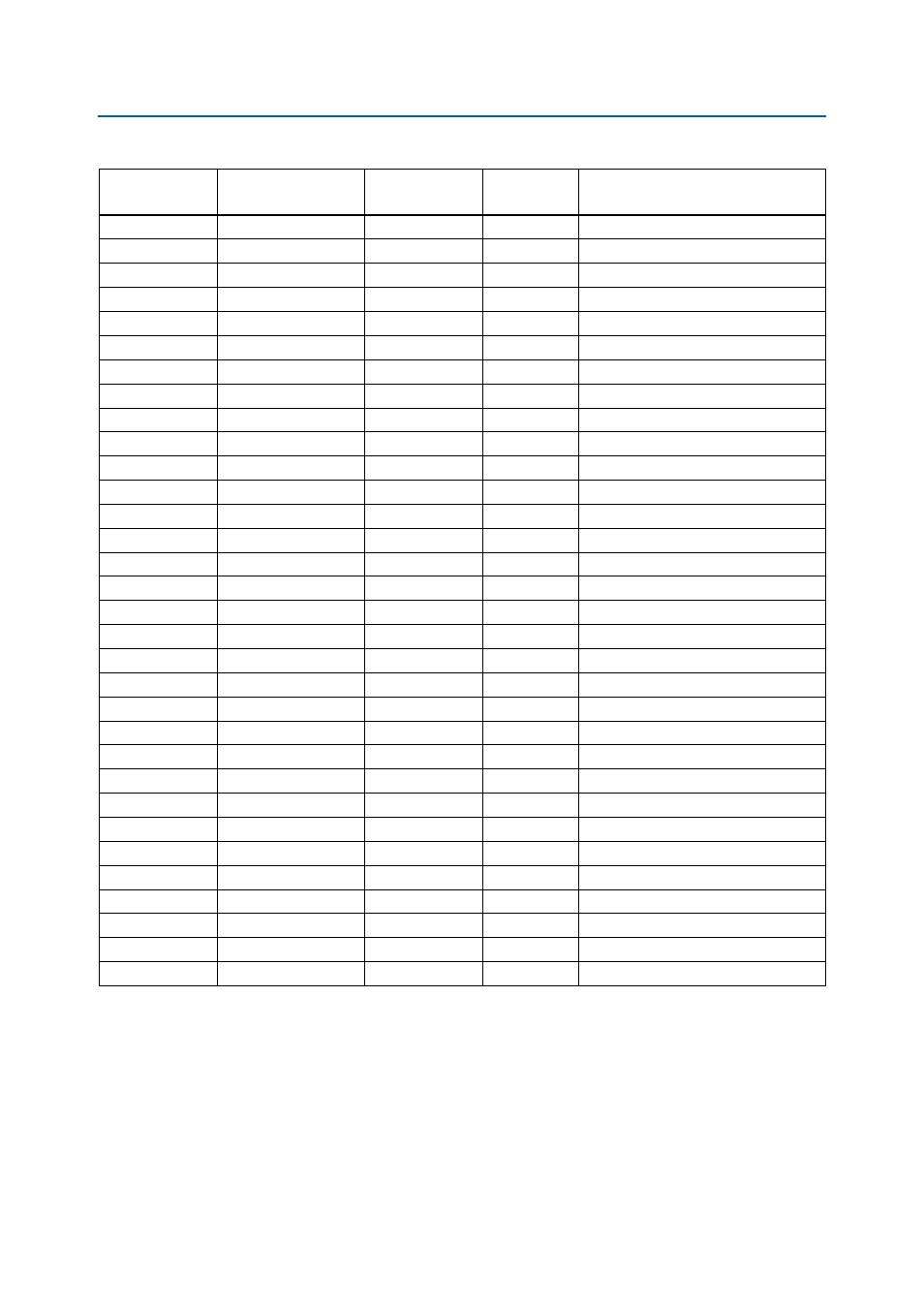
G7
FX2_FLAGB
—
3.3-V
Slave FIFO output status
H8
FX2_FLAGC
—
3.3-V
Slave FIFO output status
G6
FX2_PA1
—
3.3-V
USB 2.0 PHY port A interface
F8
FX2_PA2
—
3.3-V
USB 2.0 PHY port A interface
F7
FX2_PA3
—
3.3-V
USB 2.0 PHY port A interface
F6
FX2_PA4
—
3.3-V
USB 2.0 PHY port A interface
C8
FX2_PA5
—
3.3-V
USB 2.0 PHY port A interface
C7
FX2_PA6
—
3.3-V
USB 2.0 PHY port A interface
C6
FX2_PA7
—
3.3-V
USB 2.0 PHY port A interface
H3
FX2_PB0
—
3.3-V
USB 2.0 PHY port B interface
F4
FX2_PB1
—
3.3-V
USB 2.0 PHY port B interface
H4
FX2_PB2
—
3.3-V
USB 2.0 PHY port B interface
G4
FX2_PB3
—
3.3-V
USB 2.0 PHY port B interface
H5
FX2_PB4
—
3.3-V
USB 2.0 PHY port B interface
G5
FX2_PB5
—
3.3-V
USB 2.0 PHY port B interface
F5
FX2_PB6
—
3.3-V
USB 2.0 PHY port B interface
H6
FX2_PB7
—
3.3-V
USB 2.0 PHY port B interface
A8
FX2_PD0
—
3.3-V
USB 2.0 PHY port D interface
A7
FX2_PD1
—
3.3-V
USB 2.0 PHY port D interface
B6
FX2_PD2
—
3.3-V
USB 2.0 PHY port D interface
A6
FX2_PD3
—
3.3-V
USB 2.0 PHY port D interface
B3
FX2_PD4
—
3.3-V
USB 2.0 PHY port D interface
A3
FX2_PD5
—
3.3-V
USB 2.0 PHY port D interface
C3
FX2_PD6
—
3.3-V
USB 2.0 PHY port D interface
A2
FX2_PD7
—
3.3-V
USB 2.0 PHY port D interface
B8
FX2_RESETN
V21
3.3-V
Embedded USB-Blaster hard reset
F3
FX2_SCL
—
3.3-V
USB 2.0 PHY serial clock
G3
FX2_SDA
—
3.3-V
USB 2.0 PHY serial data
A1
FX2_SLRDN
—
3.3-V
Read strobe for slave FIFO
B1
FX2_SLWRN
—
3.3-V
Write strobe for slave FIFO
B7
FX2_WAKEUP
—
3.3-V
USB 2.0 PHY wake signal
G2
USB_CLK
AA23
3.3-V
USB 2.0 PHY 48-MHz interface clock
Table 2–5. USB 2.0 PHY Schematic Signal Names and Functions (Part 2 of 2)
Board Reference
(U18)
Schematic
Signal Name
Cyclone V E
FPGA Pin Number
I/O Standard
Description