Off-board clock input/output, General user input/output, User-defined push buttons – Altera Cyclone V E FPGA Development Board User Manual
Page 28: Off-board clock input/output –20, General user input/output –20, User-defined push buttons –20
2–20
Chapter 2: Board Components
General User Input/Output
Cyclone V E FPGA Development Board
March 2013
Altera Corporation
Reference Manual
Off-Board Clock Input/Output
The development board has input and output clocks which can be driven onto the
board. The output clocks can be programmed to different levels and I/O standards
according to the FPGA device’s specification.
Table 2–11
lists the clock inputs for the development board.
Table 2–12
lists the clock outputs for the development board.
General User Input/Output
This section describes the user I/O interface to the FPGA, including the push buttons,
DIP switches, LEDs, and character LCD.
User-Defined Push Buttons
The development board includes three user-defined push buttons. For information on
the system and safe reset push buttons, refer to
.
Board references S5, S6, S7, and S8 are push buttons for controlling the FPGA designs
that loads into the Cyclone V E FPGA device. When you press and hold down the
switch, the device pin is set to logic 0; when you release the switch, the device pin is
set to logic 1. There are no board-specific functions for these general user push
buttons.
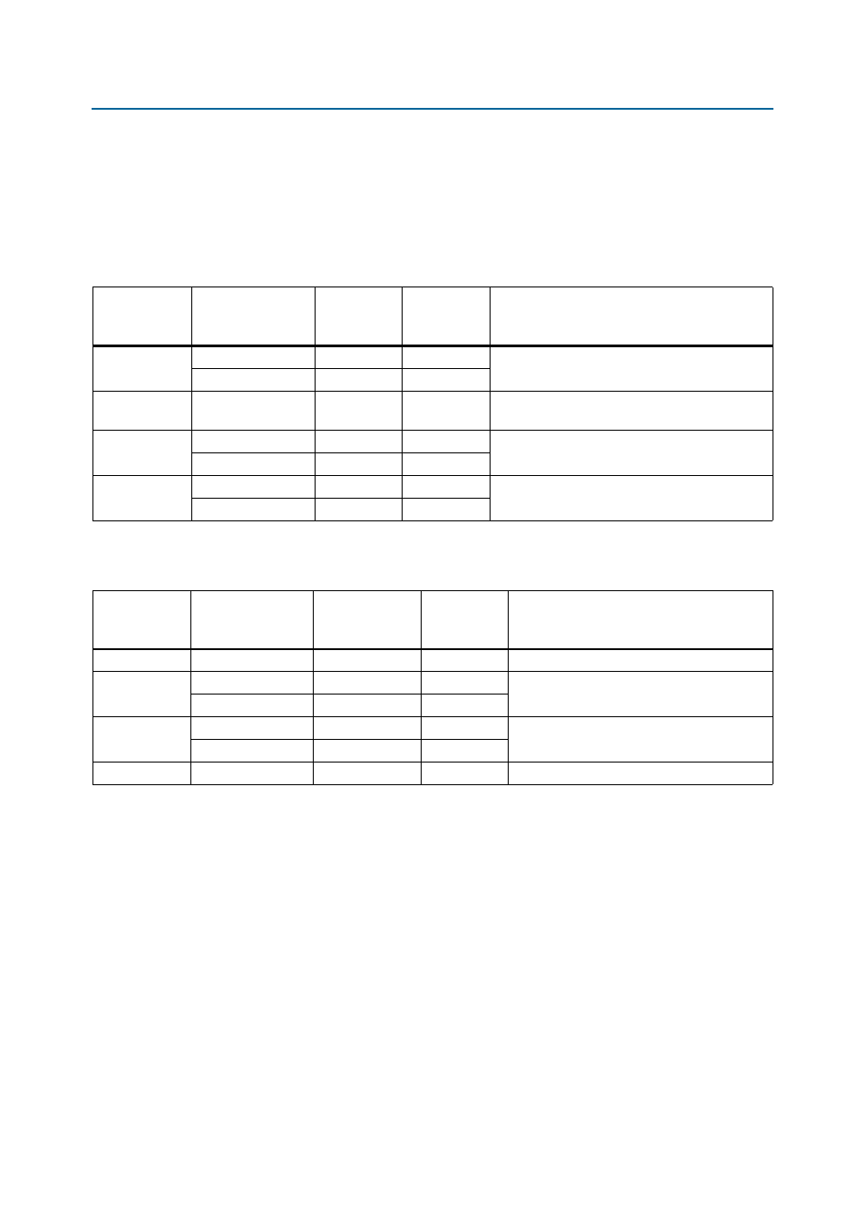
Table 2–11. Off-Board Clock Inputs
Source
Schematic Signal
Name
I/O Standard
Cyclone V E
FPGA Pin
Number
Description
SMA
CLKIN_SMA_P
LVDS
—
Input to LVDS fan-out buffer.
CLKIN_SMA_N
LVDS
—
Samtec HSMC
HSMA_CLK_IN0
2.5-V
AB16
Single-ended input from the installed HSMC cable
or board.
Samtec HSMC
HSMA_CLK_IN_P1
LVDS/2.5-V
AB14
LVDS input from the installed HSMC cable or
board. Can also support 2x LVTTL inputs.
HSMA_CLK_IN_N1
LVDS/LVTTL
AC14
Samtec HSMC
HSMA_CLK_IN_P2
LVDS/LVTTL
Y15
LVDS input from the installed HSMC cable or
board. Can also support 2x LVTTL inputs.
HSMA_CLK_IN_N2
LVDS/LVTTL
AA15
Table 2–12. Off-Board Clock Outputs
Source
Schematic Signal
Name
I/O Standard
Cyclone V E
FPGA Pin
Number
Description
Samtec HSMC
HSMA_CLK_OUT0
2.5V CMOS
AJ14
FPGA CMOS output (or GPIO)
Samtec HSMC
HSMA_CLK_OUT_P1
LVDS/2.5V CMOS
AE22
LVDS output. Can also support 2x CMOS
outputs.
HSMA_CLK_OUT_N1
LVDS/2.5V CMOS
AF23
Samtec HSMC
HSMA_CLK_OUT_P2
LVDS/2.5V CMOS
AG23
LVDS output. Can also support 2x CMOS
outputs.
HSMA_CLK_OUT_N2
LVDS/2.5V CMOS
AH22
SMA
CLKOUT_SMA
2.5V CMOS
F9
FPGA CMOS output (or GPIO)