Lpddr2 sdram, Lpddr2 sdram –35 – Altera Cyclone V E FPGA Development Board User Manual
Page 43
Chapter 2: Board Components
2–35
Memory
March 2013
Altera Corporation
Cyclone V E FPGA Development Board
Reference Manual
LPDDR2 SDRAM
The LPDDR2 is a mobile low-power DDR2 SDRAM device that operates at 1.2 V. This
interface connects to the horizontal I/O banks on the top edge of the FPGA device.
The device speed is 300 MHz. Only x16 configuration is used although the LPDDR2
SDRAM on the board is a x32 device.
lists the LPDDR2 SDRAM pin assignments, signal names, and functions.
The signal names and types are relative to the Cyclone V E FPGA in terms of I/O
setting and direction.
C2
DDR3_DQ25
D17
1.5-V SSTL Class I
Data bus byte lane 3
D7
DDR3_DQ26
C12
1.5-V SSTL Class I
Data bus byte lane 3
A7
DDR3_DQ27
E17
1.5-V SSTL Class I
Data bus byte lane 3
A3
DDR3_DQ28
C16
1.5-V SSTL Class I
Data bus byte lane 3
C3
DDR3_DQ29
A14
1.5-V SSTL Class I
Data bus byte lane 3
B8
DDR3_DQ30
D12
1.5-V SSTL Class I
Data bus byte lane 3
C8
DDR3_DQ31
A13
1.5-V SSTL Class I
Data bus byte lane 3
F3
DDR3_DQS_P2
K16
Differential 1.5-V
SSTL Class I
Data strobe P byte lane 2
G3
DDR3_DQS_N2
L16
Differential 1.5-V
SSTL Class I
Data strobe N byte lane 2
C7
DDR3_DQS_P3
K17
Differential 1.5-V
SSTL Class I
Data strobe P byte lane 3
B7
DDR3_DQS_N3
J17
Differential 1.5-V
SSTL Class I
Data strobe N byte lane 3
K1
DDR3_ODT
H19
1.5-V SSTL Class I
On-die termination enable
J3
DDR3_RASN
A24
1.5-V SSTL Class I
Row address select
T2
DDR3_RESETN
L19
1.5-V SSTL Class I
Reset
L3
DDR3_WEN
B22
1.5-V SSTL Class I
Write enable
L8
DDR3_ZQ2
—
1.5-V SSTL Class I
ZQ impedance calibration
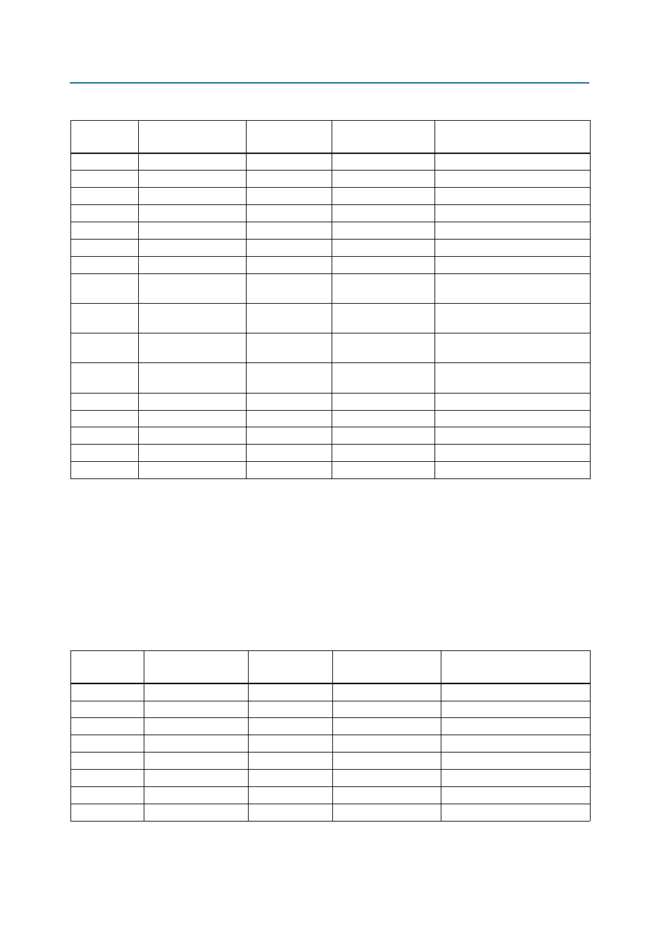
Table 2–24. DDR3 Device Pin Assignments, Schematic Signal Names, and Functions (Part 4 of 4)
Board
Reference
Schematic
Signal Name
Cyclone V E FPGA
Pin Number
I/O Standard
Description
Table 2–25. LPDDR2 SDRAM Schematic Signal Names and Functions
Board
Reference (U9)
Schematic
Signal Name
Cyclone V E
FPGA Pin Number
I/O Standard
Description
AC6
LPDDR2_CA0
Y30
1.2-V HSUL
Address bus
AB6
LPDDR2_CA1
T30
1.2-V HSUL
Address bus
AC7
LPDDR2_CA2
W29
1.2-V HSUL
Address bus
AB8
LPDDR2_CA3
AB29
1.2-V HSUL
Address bus
AB9
LPDDR2_CA4
W30
1.2-V HSUL
Address bus
W1
LPDDR2_CA5
U29
1.2-V HSUL
Address bus
V2
LPDDR2_CA6
AC30
1.2-V HSUL
Address bus
U1
LPDDR2_CA7
R30
1.2-V HSUL
Address bus