Altera Stratix III Development Board User Manual
Page 11
Chapter 2: Board Components
2–3
Board Overview
May 2013
Altera Corporation
Stratix III 3SL150 Development Board
Reference Manual
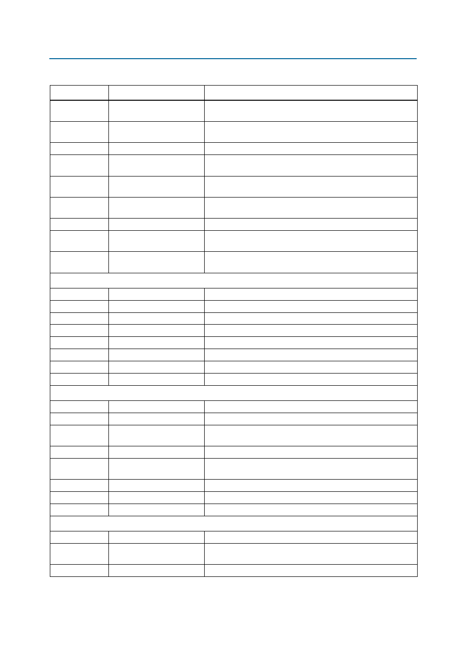
D6, D7, D8
Ethernet PHY LEDs
Green Ethernet PHY LEDs. Illuminate when Ethernet PHY is using the
10/100/1000 Mbps (D6, D7, D8) connection speeds.
D9
Duplex Ethernet PHY LED
Green Ethernet PHY LED. Illuminates when Ethernet PHY is both
sending and receiving data.
D16
Power LED
Blue LED indicates when power is applied to the board.
D14, D15
Ethernet PHY transmit/receive
activity LEDs
Green LEDs. Illuminates when transmit/receive data is active from the
Ethernet PHY.
SW2
MAX II Control DIP switch
Controls various features of the MAX II device specific to the Stratix III
development board.
SW1
JTAG control DIP switch
JTAG control DIP switch used to remove or include devices in the
active JTAG chain.
U27
Power display
Displays power measured by the MAX II CPLD.
D11, D12
HSMC Port A transmit/receive
activity LEDs
Illuminates when transmit/receive data is active from the HSMC Port A.
D2, D3
HSMC Port B transmit/receive
activity LEDs
Illuminates when transmit/receive data is active from the HSMC Port B.
Clock Circuitry
Y1
125 MHz
MAX II 125-MHz device clock.
Y2
24-MHz crystal
Cypress USB PHY.
Y3
6-MHz crystal
USB PHY FTDI reference clock.
Y4
24 MHz
MAX II 24-MHz device clock.
Y5
125 MHz
125-MHz clock oscillator used for the system clock.
Y6
50 MHz
50-MHz clock oscillator used for data processing.
J16
SMA clock input
SMA connector that allows the provision of an external clock input.
J17
SMA clock output
SMA connector that allows the provision of an external clock output.
General User Input and Output
S2 through S5
User push-buttons
Four 2.5-V push-button switches for user-defined, logic inputs.
S6
CPU reset push-button
One 2.5-V push-button switch for FPGA logic and CPU reset.
S1 and S7
Reset and factory
configuration push-button
Two 2.5-V push-button switches that control FPGA configuration from
flash memory.
D20 through D27
User LEDs
Eight user-defined LEDs.
SW3
PGM Config Select rotary
switch
Rotary switch to select which FPGA configuration file is loaded from
the flash device into the FPGA.
SW6
Power Select rotary switch
Power rail select for on-board power monitor.
U28
User display
User-defined, green 7-segment display.
SW5
User DIP switch
User-defined, eight position DIP switch.
Memory
U9
Flash
512 Mbits of flash memory.
U4, U10
P-SRAM
The P-SRAM devices connect to the MAX II device as well as the flash
memory device.
U17, U20
DDR2 SDRAM
Two 16M × 8, 1.8-V core devices in 60-pin FBGA packages.
Table 2–1. Stratix III Development Board (Part 2 of 3)
Board Reference
Type
Description