Max ii cpld, Max ii cpld –8 – Altera Stratix III Development Board User Manual
Page 16
2–8
Chapter 2: Board Components
MAX II CPLD
Stratix III 3SL150 Development Board
May 2013
Altera Corporation
Reference Manual
MAX II CPLD
The board utilizes an Altera MAX II CPLD (U5) for the following purposes:
■
Power-up configuration of the FPGA from flash memory
■
Embedded USB-Blaster core for USB-based configuration of the FPGA
■
Power consumption monitoring and display
Additionally, the MAX II device is also used to help dual-footprint the FTDI USB
device and Cypress USB device. Each device has a shared path between the USB
device and the MAX II CPLD. This path then drives to the FPGA separately.
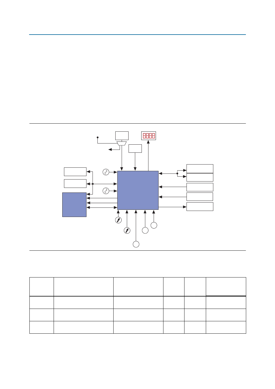
illustrates the MAX II device’s functional block diagram.
lists the I/O signals present on the MAX II CPLD. The signal names and
functions are relative to the MAX II device (U5).
Figure 2–5. MAX II Device’s Block Diagram
Cypress 480 Mb/s
USB (x16)
FTDI
12 Mb/s USB (x8)
Config Status
LEDs
8-MB
SRAM (x32)
64-MB
Flash (x16)
MAX II CPLD
JTAG
Header
24 MHz
MAX II Device
Control DIP Switch
Power Display
RESET_CONFIG
PB CPU_RESET
PB
FACTORY_CONFIG
PB
PWR_SEL
JTAG Control
DIP Switch
Stratix III
Device
PS Config
JTAG Config
USB Data Bus
PGM_CONFIG_SEL
Power
Measure
1.8-V CMOS
1.8-V CMOS
1.8-V CMOS
2.5-V CMOS
2.5-V CMOS
2.5-V CMOS
To FPGA
1.8-V CMOS
FSM Bus
125 MHz
Table 2–5. MAX II Device Pin-out (Part 1 of 9)
MAX II
Pin Number
Description
Schematic Signal Name
I/O
Standard
Stratix III
Pin
Number
Other Connections
N9
Address bus shared with flash
and P-SRAM bit 0
FSM_A0
1.8 V
F22
U9 pin A1
T8
Address bus shared with flash
and P-SRAM bit 1
FSM_A1
1.8 V
H23
U9 pin B1 and U4 pin
A3 and U10 pin A3
T9
Address bus shared with flash
and P-SRAM bit 2
FSM_A2
1.8 V
G23
U9 pin C1 and U4 pin
A4 and U10 pin A4