Altera Stratix III Development Board User Manual
Page 74
2–66
Chapter 2: Board Components
On-Board Memory
Stratix III 3SL150 Development Board
May 2013
Altera Corporation
Reference Manual
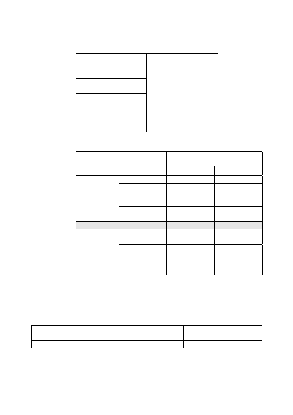
shows the flash sector map.
f
For more read and write timing specification, refer to the Intel Corporation website at
lists the flash memory device component reference and manufacturing
information.
FPGA design 7
0x034E.FFFF
0x0000.0000
FPGA design 6
FPGA design 5
FPGA design 4
FPGA design 3
FPGA design 2
FPGA design 1
FPGA design 0 (Default)
Factory design
Table 2–57. Flash Sector Map–Top and Bottom Parameter Dies
Die Stack
Configuration
Size (KBytes)
512-Mbit Flash
(2 × 256 Mbits with 1 CE)
Block
Address Range
256-Mbit Top
Parameter Die
32
517
1FFC000
–1FFFFFF
...
...
...
32
514
1FF0000
–1FF3FFF
128
513
1FE0000
–1FEFFFF
...
...
...
128
259
1000000
–100FFFF
256-Mbit Bottom
Parameter Die
128
258
770000
–77FFFF
...
...
760000
–76FFFF
128
4
...
32
3
010000
– 01FFFF
...
...
000000
–00FFFF
32
0
...
Table 2–56. Flash Memory Map (Part 2 of 2)
Name
Address
Table 2–58. Flash Memory Device Component Reference and Manufacturing Information
Board Reference
Description
Manufacturer
Manufacturing
Part Number
Manufacturer
Website
U9
512 Mbit, 1.7 to 2.0 V core, 64-pin BGA
Intel Corporation
PC48F4400P0VB00