Table 2–7 – Altera Stratix III Development Board User Manual
Page 26
2–18
Chapter 2: Board Components
Configuration, Status, and Setup Elements
Stratix III 3SL150 Development Board
May 2013
Altera Corporation
Reference Manual
■
The JTAG control switch, refer to
“JTAG Control DIP Switch” on page 2–21
.
You can use the JTAG header can be used with an external USB-Blaster cable, or
equivalent, to program either the MAX II CPLD or the Stratix III FPGA. Most users of
the Stratix III development board do not use the JTAG header at all and instead use a
USB cable along with the embedded USB-Blaster. Using an external USB-Blaster with
the JTAG header requires disabling the embedded USB-Blaster function. See
1
If complete repower is required, unplug and replug the USB cable into board
reference J5.
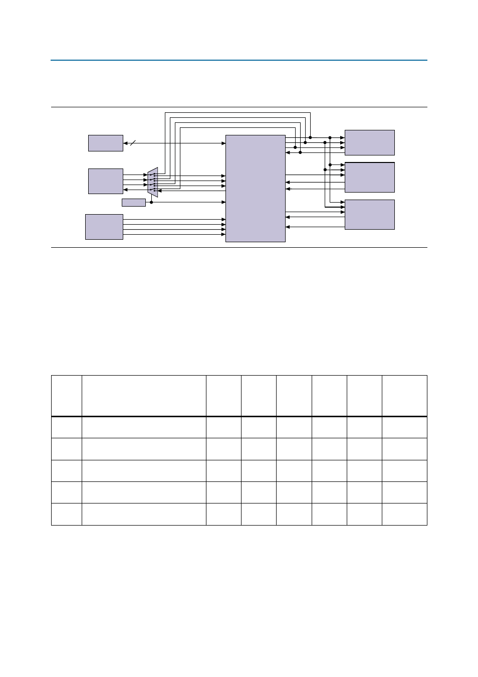
Figure 2–6. JTAG Chain with the MAX II Device and the Stratix III Device
(2.5V)
(2.5V)
(2.5V)
TDI
TDO
TMS
TCK
FPGA
TDI
TDO
TMS
TCK
MAX II
CPLD
PSNTn
TDI
TDO
TMS
TCK
PSNTn
TDI
TDO
TMS
TCK
FPGA_Bypass
HSMA_Bypass
USB 2.0
TDO
TDI
TMS
TCK
GPIO Pins
DEV_SEL
HSMA_Bypass
MAX_EN
GPIO Pins
GPIO Pins
GPIO Pins
HSMC
Port A
HSMC
Port A
HSMC
Port B
JTAG
Header
JTAG Control
DIP Switch
Jumper
Table 2–7. JTAG Settings
Number
Description
FPGA
Bypass
(SW1.1)
HSMA
Bypass
(SW1.2)
HSMB
Bypass
(SW1.3)
MAX
Enable
(SW1.4)
PFL
Enable
(SW2.5)
Device
Select
(DEV_SEL)
Jumper, J2
1
Embedded USB Blaster
Stratix III target device only
1
0
0
0
1
X
2
Embedded USB Blaster
Stratix III device + HSMC Port A
1
1
0
0
1
X
3
Embedded USB Blaster
Stratix III device + HSMC Port B
1
0
1
0
1
X
4
External USB Blaster
Stratix III target device only
X
X
X
1
1
Off
5
External USB Blaster
MAX II target device only
X
X
X
X
X
On
Notes to
:
(1) The nomenclature SW1.1 indicates board reference SW1, position 1.
(2) Requires USB cable plugged into board reference J5.
(3) Board reference SW2.5 might need to be set to off (0) for the embedded USB-Blaster to program the Stratix III FPGA.
(4) Requires external USB-Blaster or equivalent plugged into board reference J23 (PCB bottom).
(5) “1” indicates the PFL is enabled and “0” indicates the PFL is disabled.