Power supply, Power distribution system, Power supply –67 – Altera Stratix III Development Board User Manual
Page 75: Power distribution system –67
Chapter 2: Board Components
2–67
Power Supply
May 2013
Altera Corporation
Stratix III 3SL150 Development Board
Reference Manual
Power Supply
The board’s power is provided through an IBM laptop style DC power input. The
input voltage must be in the range of 14 V to 20 V. The DC voltage is then stepped
down to the various power rails used by the components on the board and installed
into the HSMC connectors.
An on-board, multi-channel A/D converter measures both voltage and current for
several specific board rails. The power utilization is displayed on either the graphics
display or the dedicated 7-segment display.
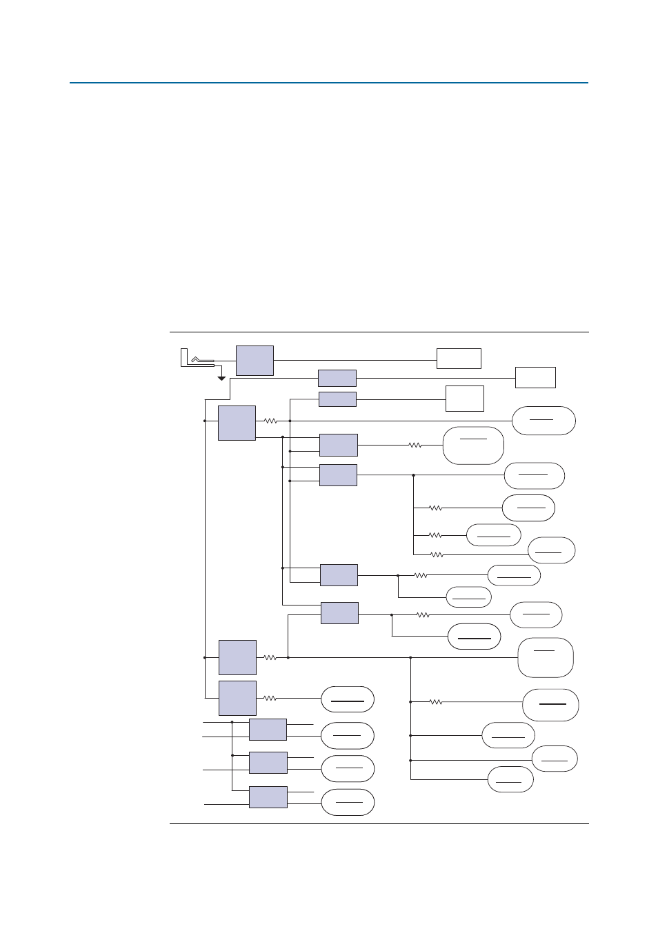
Power Distribution System
shows the power distribution system, which uses current power rails. The
currents shown reflect the regulator inefficiencies and regulator sharing.
Figure 2–20. Power Distribution System
DC INPUT
14V-20V
R
MEASURE
3.3V
Power Net
HSMC Port A, B
Flash Core, USN (FX2LP)
1 . 5 / 1 . 8 V
1 . 1 V
1 . 8 V
3 . 3 V
3 . 3 V
2 . 5 V
3 . 3 V
2 . 5 V
1 . 1 V
1 . 1 V
R MEASURE
R MEASURE
R
MEASURE
R
MEASURE
Partial Plane
CPLD VCCIO (B1, B2)
Marvell PHY, Graphics
Partial Plane
FPGA VCCIO
(B4A, B5, B6)
2.5V_B2
2.5V
Partial Plane
FPGA VCCIO (B2)
R MEASURE
2.5V_A
Power Net
VDDQ_QDRII
Partial Plane
QDRII VDDQ
Partial Plane
R MEASURE
Partial Plane
FPGA VCCPD
1 . 1 V
Partial Plane
ENET PHY DVDD
Partial Plane
FPGA VCC
FPGA_VCCD_PLL
1 . 8 V
R MEASURE
1 . 8 V
R MEASURE
Partial Plane
1 . 8 V
1 . 8 V
Partial Plane
DIMM VDD/VDDQ
Partial Plane
DEV VDD/VDDQ
1 . 8 V
Partial Plane
QDRII VDD
Power Net
R
MEASURE
1 . 1 V
VCCL
Partial Plane
FPGA VCCL
VREF_DIMM
0 . 9 V
V IN
V VLDOIN
VTT _ DIMM
Power Net
DIMM Termination
Resistors
0 . 9 V
VREF_QDRII
0 . 9 V / 0 . 75 V
V IN
V VLDOIN
V IN
V VLDOIN
VTT _ DEV
Power Net
Device Termination
Resistors
VTT _ QDRII
Power Net
QDR II Termination
Resistors
5 . 0 V
VREF_DEV
VDDQ_QDRII
3 . 3 V
1 . 8 V
5 . 0 V
BST
V IN
BST
V IN
BST
V IN
BST
V IN
1 . 8 V _ DEV
12 V Power Net
HSMC Port A, Port B,
and Graphics Display
5 V Power Net
USB - VCC (FTDI),
14-pin LCD Header
3.0V_CSENSE
Power Net
LTC 2402 A/D
ADG 725 MUX
3.3V
3.0V
5.0V
12V
Wide Input
Switching
Regulator
(LT1374)
Wide Input
Switching
Regulator
Module
(LTM4601)
Linear
(LT1761)
Linear
(LT1761)
Linear
(LT3026)
Linear
(LT3026)
1.5/1.8V
Linear
(LT3026)
Linear
(LT3026)
Wide Input
Switching
Regulator
Module
(LTM4601)
Wide Input
Switching
Regulator
Module
(LTM4601)
1.8V_DIMM
Linear
(TPS5100)
Linear
(TPS5100)
Linear
(TPS5100)
2.5V_B4a_B5_B6
FPGA VCCA PLL
FPGA VCCPT
FPGA VCC_CLKIN
FPGA_VCCPGM
2.5V_VCCPD
FPGA VCCIO (B7)
CPLD VCCINT
CPLD VCCIO (B3, B4)
PSRAM VCC.VCCD
Flash VDDQ
FPGA VCCIO (B3,B4)
FPGA VCCIO (B1, B8)
1.5V_1.8V_B7
1.8V
1.8V_S3
1.8V_DIMM
1.8V_DEV
1.8V_QDRII
1V_VCC