P-sram, P-sram –58 – Altera Stratix III Development Board User Manual
Page 66
2–58
Chapter 2: Board Components
On-Board Memory
Stratix III 3SL150 Development Board
May 2013
Altera Corporation
Reference Manual
lists the QDRII device component reference and manufacturing
information.
P-SRAM
The board features 8 MBytes of P-SRAM memory with a 32-bit data bus. The devices
use 1.8-V CMOS signaling and are optimized for low cost and power.
The 32-bit interface comprises two ×16 devices. The Samsung part features a
maximum frequency of 104 MHz (104 Mbps). The theoretical bandwidth of the entire
interface is 416 Mbps.
The P-SRAM devices are part of a shared bus with connectivity to the MAX II CPLD
as well as the flash memory, which is called the FSM bus. All three devices use 1.8-V
CMOS signaling. Altera recommends using the 5-
Ω OCT setting on the FPGA and the
one-half drive setting on the SRAM.
lists the P-SRAM interface signal name, description, and signal type.
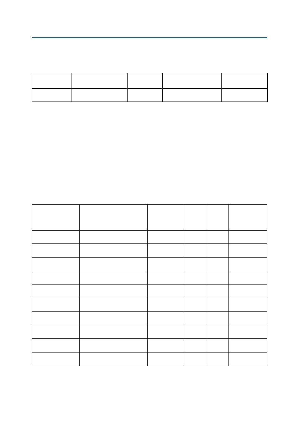
Table 2–51. QDRII Device Component Reference and Manufacturing Information
Board Reference
Description
Manufacturer
Manufacturing
Part Number
Manufacturer
Website
U15
400 MHz QDRII+ burst-of-4
device for 2M × 18
Cypress
Semiconductor
CY7C1263V18-400BZXCES
Table 2–52. P-SRAM Device Pin-Out (Part 1 of 4)
Board Reference
Description
Schematic
Signal Name
I/O
Standard
Stratix III
Device
Pin
Number
Other
Connections
U4 and U10 pin A3
Address bus shared with flash
and P-SRAM bit 1
FSM_A1
1.8 V
H23
U5 pin T8 and U9
pin B1
U4 and U10 pin A4
Address bus shared with flash
and P-SRAM bit 2
FSM_A2
1.8 V
G23
U5 pin T9 and U9
pin C1
U4 and U10 pin A5
Address bus shared with flash
and P-SRAM bit 3
FSM_A3
1.8 V
F23
U5 pin R9 and U9
pin D1
U4 and U10 pin B3
Address bus shared with flash
and P-SRAM bit 4
FSM_A4
1.8 V
D27
U5 pin P9 and U9
pin D2
U4 and U10 pin B4
Address bus shared with flash
and P-SRAM bit 5
FSM_A5
1.8 V
D28
U5 pin T10 and
U9 pin A2
U4 and U10 pin C3
Address bus shared with flash
and P-SRAM bit 6
FSM_A6
1.8 V
F25
U5 pin P13 and
U9 pin C2
U4 and U10 pin C4
Address bus shared with flash
and P-SRAM bit 7
FSM_A7
1.8 V
F26
U5 pin R10 and
U9 pin A3
U4 and U10 pin D4
Address bus shared with flash
and P-SRAM bit 8
FSM_A8
1.8 V
G24
U5 pin M10 and
U9 pin B3
U4 and U10 pin H2
Address bus shared with flash
and P-SRAM bit 9
FSM_A9
1.8 V
F24
U5 pin M11 and
U9 pin C3
U4 and U10 pin H3
Address bus shared with flash
and P-SRAM bit 10
FSM_A10
1.8 V
E26
U5 pin N10 and
U9 pin C4