Altera Stratix III Development Board User Manual
Page 69
Chapter 2: Board Components
2–61
On-Board Memory
May 2013
Altera Corporation
Stratix III 3SL150 Development Board
Reference Manual
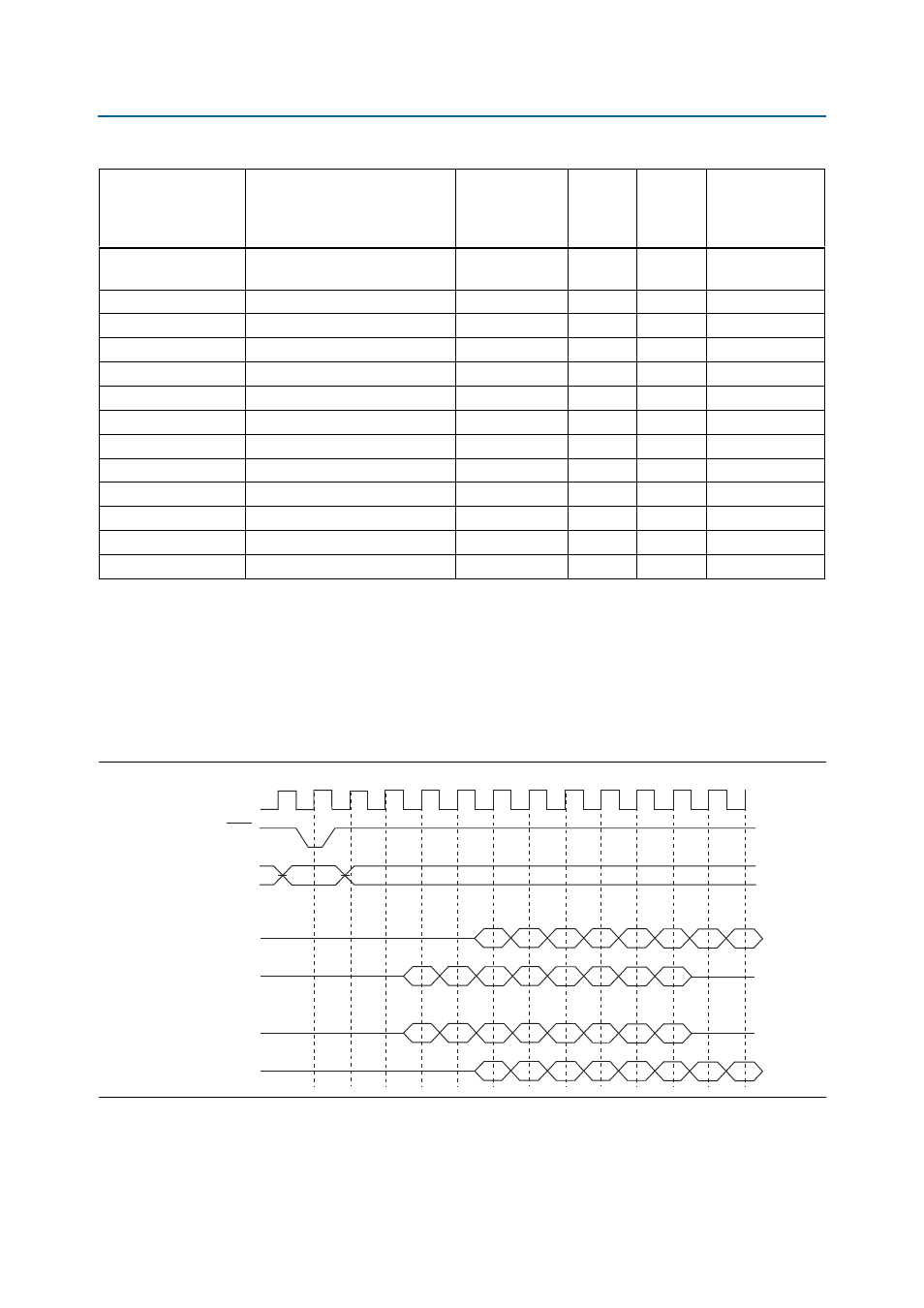
illustrates the latency for both fixed and variable modes of operation. For
asynchronous accesses, each of the two devices has its own WAIT pin wired to the
Stratix III device.
f
For Samsung SRAM pin definitions, data sheet, and other related documentation,
refer to the Samsun
U10 pin G1
Data bus shared with flash and
P-SRAM bit 31
FSM_D31
1.8 V
B28
U5 pin C15
U10 and U4 pin J3
Address valid
SRAM_ADVn
1.8 V
D21
—
U4 pin A1
Byte write select bit 0
SRAM_BEn0
1.8 V
D22
—
U4 pin B2
Byte write select bit 1
SRAM_BEn1
1.8 V
E22
—
U10 pin A1
Byte write select bit 2
SRAM_BEn2
1.8 V
E20
—
U10 pin B2
Byte write select bit 3
SRAM_BEn3
1.8 V
H20
—
U10 and U4 pin J2
Clock
SRAM_CLK
1.8 V
C21
—
U10 and U4 pin B5
Chip select
SRAM_CSn
1.8 V
A21
—
U10 and U4 pin A2
Output enable
SRAM_OEn
1.8 V
A22
—
U10 and U4 pin A6
Power save mode
SRAM_PSn
1.8 V
AL18
—
U4 pin J1
Data wait
SRAM_WAIT0
1.8 V
G20
—
U10 pin J1
Data wait
SRAM_WAIT1
1.8 V
F20
—
U10 and U4 pin G5
Write enable
SRAM_WEn
1.8 V
B22
—
Table 2–52. P-SRAM Device Pin-Out (Part 4 of 4)
Board Reference
Description
Schematic
Signal Name
I/O
Standard
Stratix III
Device
Pin
Number
Other
Connections
Figure 2–17. SRAM Latency Timing Illustration
1st
Clock
Address
Data Out
Data In
Data In/Out
Data Out
Latency 4 (Burst Length: 8)
Latency 4 (Burst Length: 8)
Fixed Latency - A18[0]
Variable Latency - A18[1]
Latency 2 (Burst Length: 8)
Latency 2 (Burst Length: 8)
2nd
3rd
4th
5th
D0
D1
D2
6th
7th
8th
9th
10th 11th
D3
D4
D5
D6
D7
D0
D1
D2
D3
D4
D5
D6
D7
Q0
Q1
Q2
Q3
Q4
Q5
Q6
Q7
DQ0
DQ1
DQ2
DQ3
DQ4
DQ5
DQ6
DQ7
ADV