Altera Stratix III Development Board User Manual
Page 73
Chapter 2: Board Components
2–65
On-Board Memory
May 2013
Altera Corporation
Stratix III 3SL150 Development Board
Reference Manual
shows the flash on-board memory map. The memory needs to provide
non-volatile storage of a minimum of eight FPGA bit streams as well as various
settings data used for on-board devices such as Ethernet TCP/IP defaults, PFL
configuration bits, and data on the board itself. The remaining area is designated as
user flash area for storage of software binaries and other data relevant to a user FPGA
design.
U9 pin F3
Data bus shared with
flash and P-SRAM bit 10
FSM_D10
1.8 V
A26
U5 pin M6 and U4 pin C2
U9 pin F4
Data bus shared with
flash and P-SRAM bit 11
FSM_D11
1.8 V
B25
U5 pin R5 and U4 pin D2
U9 pin F5
Data bus shared with
flash and P-SRAM bit 12
FSM_D12
1.8 V
A25
U5 pin P7 and U4 pin E2
U9 pin H5
Data bus shared with
flash and P-SRAM bit 13
FSM_D13
1.8 V
J20
U5 pin T5 and U4 pin F2
U9 pin G7
Data bus shared with
flash and P-SRAM bit 14
FSM_D14
1.8 V
K20
U5 pin N7 and U4 pin F1
U9 pin E7
Data bus shared with
flash and P-SRAM bit 15
FSM_D15
1.8 V
K21
U5 pin R6 and U4 pin G1
U9 pin E6
Clock
FLASH_CLK
1.8 V
K24
U5 pin L15
U9 pin F6
Address valid
FLASH_ADVn
1.8 V
C7
U5 pin L13
U9 pin B4
Chip enable
FLASH_CEn
1.8 V
K25
U5 pin K14
U9 pin F8
Output enable
FLASH_OEn
1.8 V
K23
U5 pin M16
U9 pin F7
Ready/busy
FLASH_RDYBSYn
1.8 V
L16
U5 pin L11
U9 pin D4
Reset
FLASH_RESETn
1.8 V
E13
U5 pin M15
U9 pin G8
Write enable
FLASH_WEn
1.8 V
L22
U5 pin L12
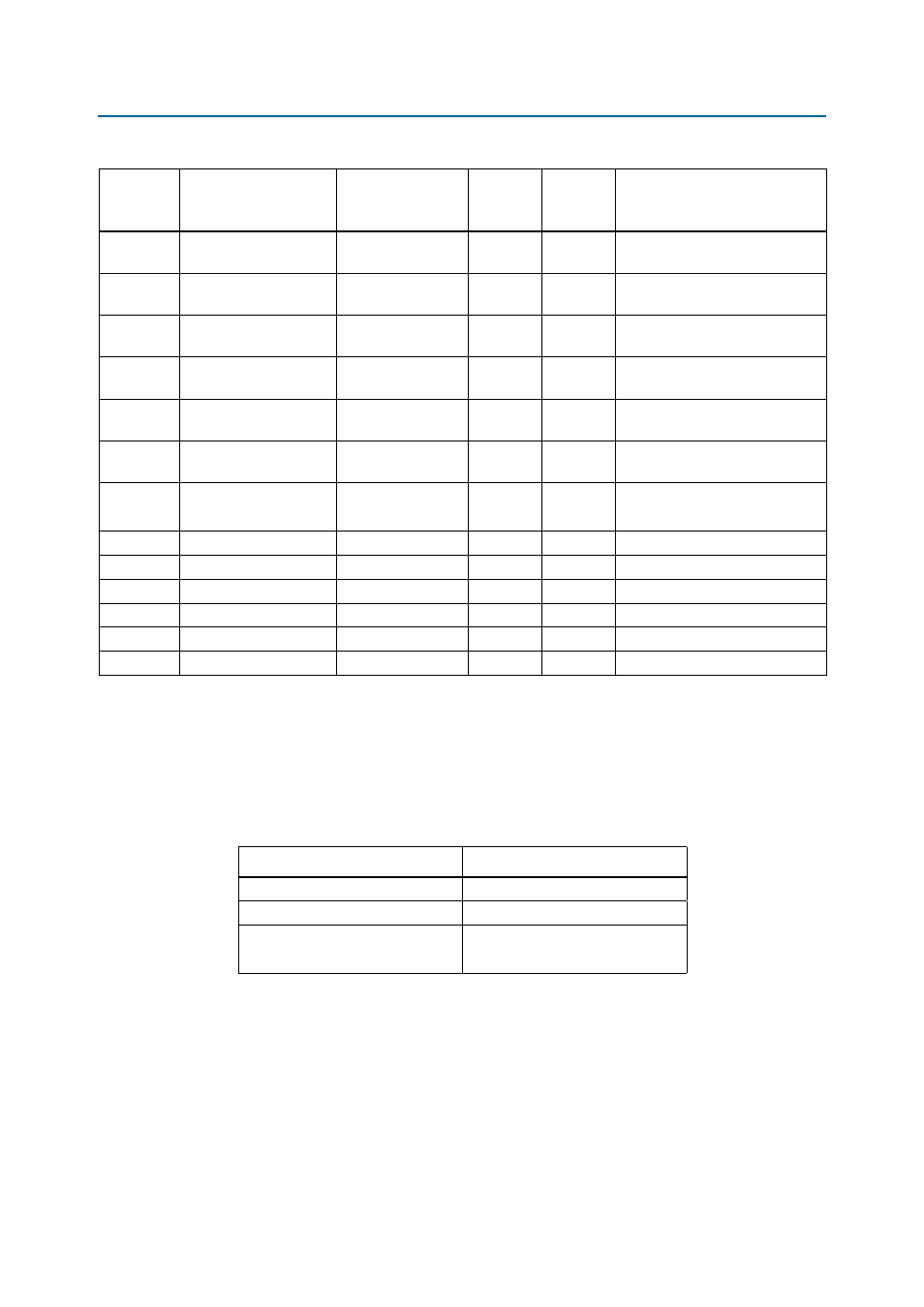
Table 2–55. Flash Interface I/O (Part 3 of 3)
Board
Reference
Description
Schematic Signal
Name
I/O
Standard
Stratix III
Pin
Number
Other Connections
Table 2–56. Flash Memory Map (Part 1 of 2)
Name
Address
PFL option bits
0x03FE.0000
Ethernet option bits
0x03FC.0000
User space (10 MBytes)
0x03FB.FFFF
0x0350.0000