Altera Stratix III Development Board User Manual
Page 15
Chapter 2: Board Components
2–7
Featured FPGA (U22)
May 2013
Altera Corporation
Stratix III 3SL150 Development Board
Reference Manual
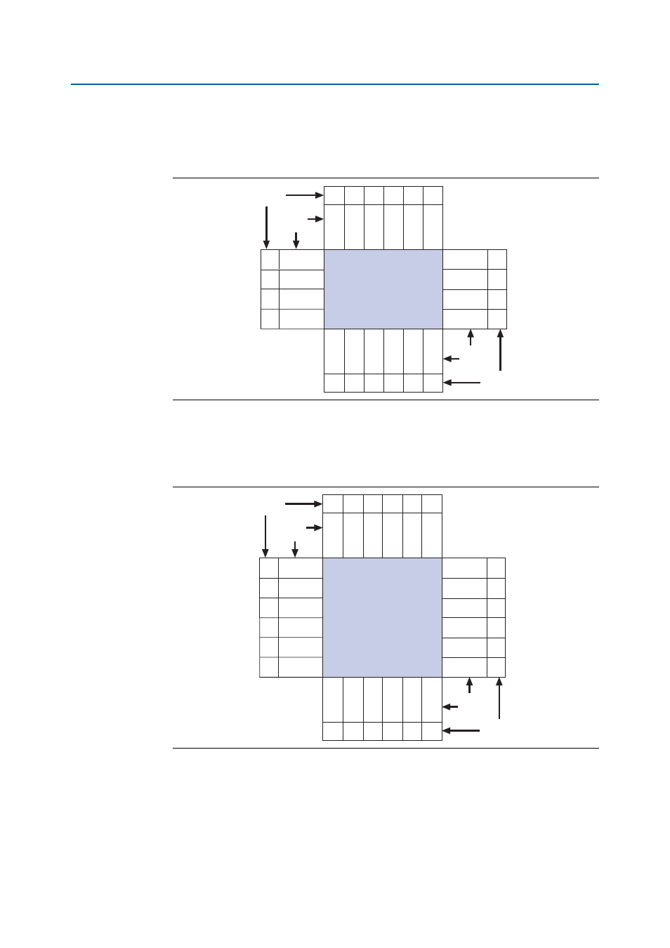
shows the configuration of the 20 user I/O banks and each bank’s I/O count
for the EP3SL150 device. Incidentally, within the same package, the EP3SL150 and the
EP3SL340 devices have the same number of PLLs, user I/O banks, and user I/Os.
shows the configuration of the 24 possible user I/O banks and each bank’s
I/O count for the EP3SL340 device in its largest package. Banks 1B, 2B, 5B, and 6B are
not available in the F1152 package.
Figure 2–3. EP3SL150F1152 Device I/O Bank Resources
Figure 2–4. EP3SL340F1517 Device I/O Bank Diagram
Bank 7A
40
Bank 7B
24
Bank 7C
32
Bank 8C
32
Bank 1A
48
Bank 1C
EP3SL150
Bank
Name
Number
of I/Os
Bank
Name
Number
of I/Os
40
Bank 2C
40
Bank 2A
Bank 6A
Bank 6C
Bank 5C
Bank 5A
48
48
40
40
48
Bank 8B
24
Bank 8A
40
Bank 4A
40
Bank 4B
24
Bank 4C
32
Bank 3C
32
Bank 3B
24
Bank 3A
40
Bank 7A
48
Bank 7B
48
Bank 7C
48
Bank 8C
48
Bank 1A
48
Bank 1B
EP3SL340
Bank
Name
Number
of I/Os
Bank
Name
Number
of I/Os
36
Bank 1C
48
Bank 2C
Bank 6A
Bank 6B
Bank 5C
Bank 5C
48
48
36
48
48
Bank 5B
36
Bank 2B
36
Bank 2A
48
Bank 5A
48
Bank 8B
48
Bank 8A
48
Bank 4A
48
Bank 4B
48
Bank 4C
48
Bank 3C
48
Bank 3B
48
Bank 3A
48