Qdrii+ sram, Qdrii+ sram –55 – Altera Stratix III Development Board User Manual
Page 63
Chapter 2: Board Components
2–55
On-Board Memory
May 2013
Altera Corporation
Stratix III 3SL150 Development Board
Reference Manual
QDRII+ SRAM
The board uses a burst-of-4 QDRII memory device for high-speed, low-latency
memory access. The interface provides addressing for a 72-Mbit device. The actual
device used may be 18, 36, or 72 Mbits. Because the Stratix III device supports
18 DQ/DQS group, the board uses a ×18 QDRII or QDRII+ SRAM device. QDRII+
SRAM is needed to support a QDRII rate that is greater than 300 MHz.
QDRII has separate read and write data ports with DDR interfaces operating up to
300 MHz. QDRII+ has separate read and write data ports with DDR interfaces
operating up to 350 MHz. Burst-of-2 devices have a DDR address bus allowing for
different read and write addresses on every clock (two data words per clock).
Burst-of-4 devices have higher data rates due to the longer sequential addressing.
U20 pin L2
Address bit 12
DDR2_DEVB_A12
SSTL-18 class I
U22-V32
U20 pin L8
Address bit 13
DDR2_DEVB_A13
SSTL-18 class I
U22-R28
U20 pin L3
Address bit 14
DDR2_DEVB_A14
SSTL-18 class I
U22-T30
U20 pin G2
Bank address bit 0
DDR2_DEVB_BA0
SSTL-18 class I
U22-N32
U20 pin G3
Bank address bit 1
DDR2_DEVB_BA1
SSTL-18 class I
U22-N33
U20 pin G1
Bank address bit 2
DDR2_DEVB_BA2
SSTL-18 class I
U22-R30
U20 pin C8
Data bit 0
DDR2_DEVB_DQ0
SSTL-18 class I
U22-P29
U20 pin C2
Data bit 1
DDR2_DEVB_DQ1
SSTL-18 class I
U22-P32
U20 pin D7
Data bit 2
DDR2_DEVB_DQ2
SSTL-18 class I
U22-N30
U20 pin D3
Data bit 3
DDR2_DEVB_DQ3
SSTL-18 class I
U22-N31
U20 pin D1
Data bit 4
DDR2_DEVB_DQ4
SSTL-18 class I
U22-R26
U20 pin D9
Data bit 5
DDR2_DEVB_DQ5
SSTL-18 class I
U22-P28
U20 pin B1
Data bit 6
DDR2_DEVB_DQ6
SSTL-18 class I
U22-R25
U20 pin B9
Data bit 7
DDR2_DEVB_DQ7
SSTL-18 class I
U22-N29
U20 pin A8
Data strobe
DDR2_DEVB_DQS_N
SSTL-18 class I
U22-L34
U20 pin B7
Data strobe
DDR2_DEVB_DQS_P
SSTL-18 class I
U22-M33
U20 pin F8
Differential output clock
DDR2_DEVB_CK_N
SSTL-18 class I
U22-R32
U20 pin E8
Differential output clock
DDR2_DEVB_CK_P
SSTL-18 class I
U22-P31
U20 pin F2
Clock enable
DDR2_DEVB_CKE
SSTL-18 class I
U22-N34
U20 pin G8
Chip select
DDR2_DEVB_CSn
SSTL-18 class I
U22-J32
U20 pin F3
Write enable
DDR2_DEVB_WEn
SSTL-18 class I
U22-T26
U20 pin G7
Column address strobe
DDR2_DEVB_CASn
SSTL-18 class I
U22-U25
U20 pin F7
Row address strobe
DDR2_DEVB_RASn
SSTL-18 class I
U22-D33
U20 pin B3
Data write mask
DDR2_DEVB_DM
SSTL-18 class I
U22-M31
U20 pin F9
On-die termination control pin DDR2_DEVB_ODT
SSTL-18 class I
U22-D34
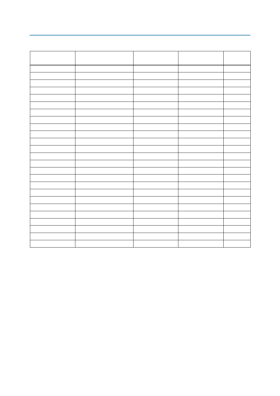
Table 2–49. DDR2 Device B Interface I/O (Part 2 of 2)
Board Reference
Description
Schematic
Signal Name
I/O
Standard
Stratix III
Pin Number