Ddr2 sdram dimm, Ddr2 sdram dimm –49 – Altera Stratix III Development Board User Manual
Page 57
Chapter 2: Board Components
2–49
On-Board Memory
May 2013
Altera Corporation
Stratix III 3SL150 Development Board
Reference Manual
DDR2 SDRAM DIMM
The board has 1 GByte DDR2 SDRAM DIMM memory interface with a 72-bit data
width on the vertical I/O banks, which is typically used as a 64-bit interface with the
additional 8 bits serving as error correction coding (ECC) bits for each of the 8-byte
lanes. The target frequency is 400 MHz (800 Mbps) with potential operation of up to
533 MHz (1,066 Mbps). The theoretical bandwidth of the entire DDR2 interface is
6,388 Mbps plus ECC, or 7,187 Mbps raw throughput.
The data interface to the FPGA fabric runs at either one-half or one-quarter the
physical layer data rate when using the Altera DDR2 MegaCore
®
function, which
equates to a doubling or quadrupling of the physical data bus width (144 bits or
288 bits, respectively). For example, a 72-bit interface with a 400-MHz external clock
speed can have a 400-MHz 144-bit internal bus or a 200-MHz 288-bit interface.
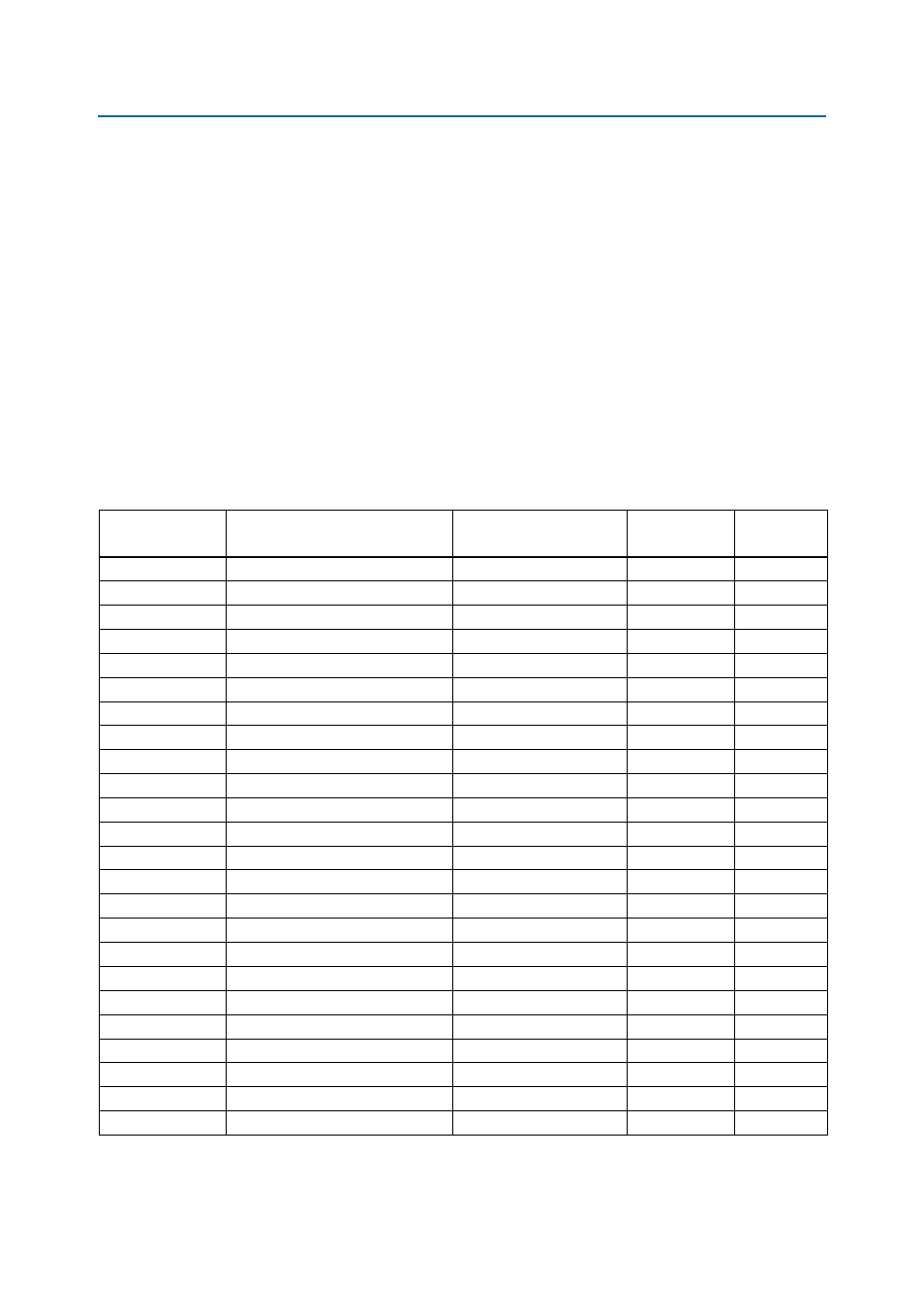
lists the DDR2 DIMM interface signals. Signal names and type are relative
to the Stratix III device regarding the I/O setting and direction. JEDEC bus widths are
used.
Table 2–45. DDR2 DIMM Interface I/O Signals (Part 1 of 4)
Board Reference
Description
Schematic
Signal Name
I/O Standard
Stratix III
Pin Number
J19 pin 188
Address bit 0
DDR2_DIMM_A0
SSTL-18 class I
AM19
J19 pin 183
Address bit 1
DDR2_DIMM_A1
SSTL-18 class I
AM18
J19 pin 63
Address bit 2
DDR2_DIMM_A2
SSTL-18 class I
AF16
J19 pin 182
Address bit 3
DDR2_DIMM_A3
SSTL-18 class I
AN16
J19 pin 61
Address bit 4
DDR2_DIMM_A4
SSTL-18 class I
AM17
J19 pin 60
Address bit 5
DDR2_DIMM_A5
SSTL-18 class I
AL19
J19 pin 180
Address bit 6
DDR2_DIMM_A6
SSTL-18 class I
AK18
J19 pin 58
Address bit 7
DDR2_DIMM_A7
SSTL-18 class I
AD16
J19 pin 179
Address bit 8
DDR2_DIMM_A8
SSTL-18 class I
AE16
J19 pin 177
Address bit 9
DDR2_DIMM_A9
SSTL-18 class I
AM16
J19 pin 70
Address bit 10
DDR2_DIMM_A10
SSTL-18 class I
AH19
J19 pin 57
Address bit 11
DDR2_DIMM_A11
SSTL-18 class I
AL16
J19 pin 176
Address bit 12
DDR2_DIMM_A12
SSTL-18 class I
AF20
J19 pin 196
Address bit 13
DDR2_DIMM_A13
SSTL-18 class I
AE23
J19 pin 174
Address bit 14
DDR2_DIMM_A14
SSTL-18 class I
AG19
J19 pin 173
Address bit 15
DDR2_DIMM_A15
SSTL-18 class I
AP12
J19 pin 71
Bank address bit 0
DDR2_DIMM_BA0
SSTL-18 class I
AN18
J19 pin 190
Bank address bit 1
DDR2_DIMM_BA1
SSTL-18 class I
AL17
J19 pin 54
Bank address bit 2
DDR2_DIMM_BA2
SSTL-18 class I
AD15
J19 pin 125
Data write mask (byte enables) bit 0
DDR2_DIMM_DM0
SSTL-18 class I
AL12
J19 pin 134
Data write mask (byte enables) bit 1
DDR2_DIMM_DM1
SSTL-18 class I
AP10
J19 pin 146
Data write mask (byte enables) bit 2
DDR2_DIMM_DM2
SSTL-18 class I
AJ15
J19 pin 155
Data write mask (byte enables) bit 3
DDR2_DIMM_DM3
SSTL-18 class I
AL22
J19 pin 202
Data write mask (byte enables) bit 4
DDR2_DIMM_DM4
SSTL-18 class I
AE22