Altera Stratix III Development Board User Manual
Page 44
2–36
Chapter 2: Board Components
General User Interfaces
Stratix III 3SL150 Development Board
May 2013
Altera Corporation
Reference Manual
f
For more information about the data sheet and related documentation, visit Lumex at
www.lumex.com
.
1
Board defaults graphics LCD interface to 80 series CPU mode and parallel interface.
You can modify these defaults by writing to the appropriate register in the MAX II
CPLD using the FSM bus.
is an excerpt from the Optrex data sheet showing the control chip in the
LCD module and illustrates the functional block diagram of the display driver. The
control chip is from New Japan Radio Corporation, part number NJU6676.
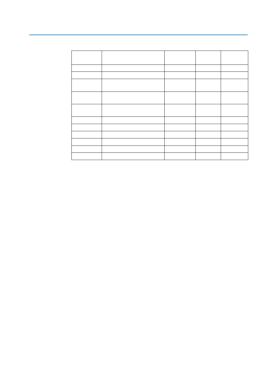
J24 pin 10
LCD data bus bit 4
OLED_DATA4
2.5 V AL32
J24 pin 11
LCD data bus bit 5
OLED_DATA5
2.5 V AB30
J24 pin 12
LCD data bus bit 6
(or SCLK)
OLED_DATA6
2.5 V
AC26
J24 pin 13
LCD data bus bit 7
(or SDATA)
OLED_DATA7
2.5 V
AA30
J24 pin 28
Parallel interface selection
(high = 68 series, low = 80 series)
OLED_BS1
2.5 V
Y26
J24 pin 1
LCD chip select
OLED_CSn
2.5 V
AE30
J24 pin 3
LCD data/command select
OLED_D_Cn
2.5 V
AD26
J24 pin 5
LCD read enable
OLED_E_RDn
2.5 V
AG31
J24 pin 2
LCD reset
OLED_RSTn
2.5 V
AP4
J24 pin 29
LCD parallel/serial data select
OLED_SERn
2.5 V
AA27
J24 pin 4
LCD write enable
OLED_WEn
2.5 V
AA31
Table 2–35. Graphics LCD Header (J24) (Part 2 of 2)
Board
Reference
Description
Schematic
Signal Name
I/O
Standard
Stratix III
Pin Number