Board overview, Board overview –2, Figure 2–1 – Altera Arria V SoC Development Board User Manual
Page 10: Table 2–1
2–2
Chapter 2: Board Components
Board Overview
July 2014
Altera Corporation
Reference Manual
Board Overview
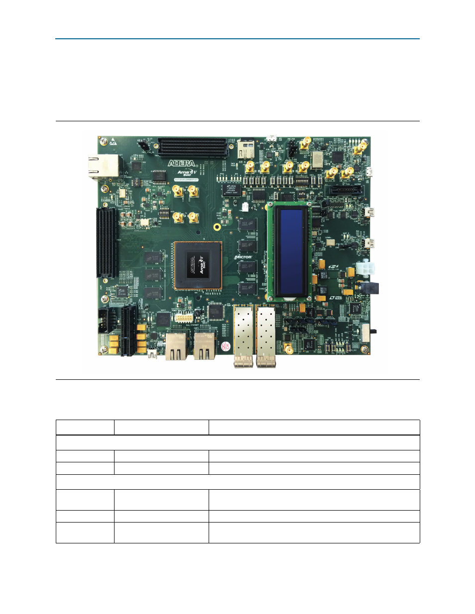
This section provides an overview of the Arria V SoC development board, including
an annotated board image and component descriptions.
shows an
overview of the board features.
describes the components and lists their corresponding board references.
Figure 2–1. Overview of the Arria V SoC Development Board
Table 2–1. Board Components (Part 1 of 3)
Board Reference
Type
Description
Featured Devices
U41
FPGA
Arria V SoC, 5ASTFD5K3F40I3, 1517-pin FBGA.
U27
CPLD
MAX V CPLD, 5M2210ZF256, 256-pin FBGA.
Configuration, Status, and Setup Elements
J35
JTAG chain header
Provides access to the JTAG chain and disables the On-board
USB-Blaster II when using an external USB-Blaster cable.
SW4
JTAG chain control DIP switch Remove or include devices in the active JTAG chain.
J50
Mini-USB header
USB interface for FPGA programming and debugging through the On-
board USB-Blaster II JTAG via a type-B USB cable.