Development board block diagram, Handling the board – Altera Arria V SoC Development Board User Manual
Page 8
1–4
Chapter 1: Overview
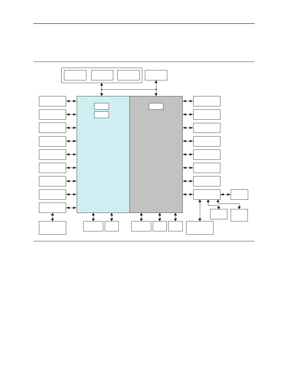
Development Board Block Diagram
July 2014
Altera Corporation
Reference Manual
Development Board Block Diagram
shows a block diagram of the Arria V SoC development board.
Handling the Board
When handling the board, it is important to observe the following static discharge
precaution:
c
Without proper anti-static handling, the board can be damaged. Therefore, use
anti-static handling precautions when touching the board.
Figure 1–1. Arria V SoC Development Board Block Diagram
DDR3 1GB
533 MHz (x32)
DDR3 1GB
533 MHz (x32)
Clock
Cleaner
Jitter
Clean Up
Buttons
Switches
LEDs
Buttons
Switches
LEDs
CSEL
BSEL
HMC
HMC
HMC
10/100 Dual
Ethernet PHY
SFP+ x2
FMC x2
MAX V
CPLD
PCIe Gen2
x4
Parallel
Configuration
Flash
DDR3 1GB
533 MHz + ECC
QSPI Flash
256 MB
Micro SD Card
USB 2.0
OTG PHY
10/100/1000
Ethernet PHY
UART to USB
UART to USB
I
2
C
Power
Management
Measurement
Serial
EPROM
RTC
2x16
Character
LCD
MAC Address
Storage
FPGA
HPS
JTAG
JTAG
USB-Blaster II
USB 2.0
MAX II
CPLD
Mictor
Connector